-
Part Symbol
-
Footprint
-
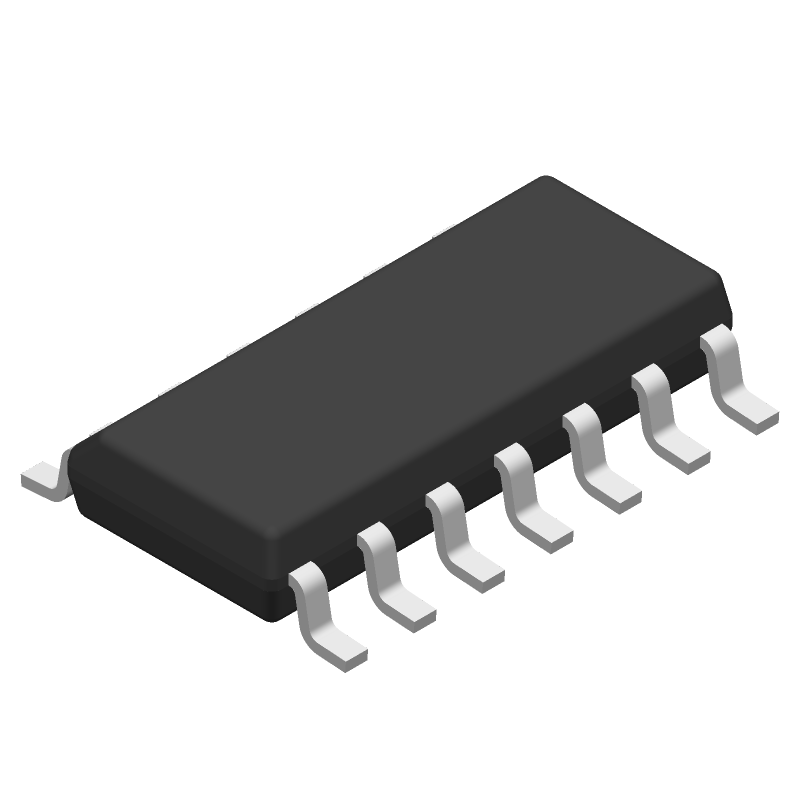
3D Model
Available Download Formats
By downloading CAD models, you agree to our Terms & Conditions and Privacy Policy

6-ch, 3-V to 18-V inverters with Schmitt-Trigger inputs 14-SOIC -55 to 125
Tip: Data for a part may vary between manufacturers. You can filter for manufacturers on the top of the page next to the part image and part number.
| Part # | Distributor | Description | Stock | Price | Buy | |
|---|---|---|---|---|---|---|
|
DISTI #
595-CD40106BM96E4
|
Mouser Electronics | Inverters Hex Schmitt Trigger RoHS: Compliant | 4416 |
|
$0.2070 / $0.6300 | Buy Now |
By downloading CAD models, you agree to our Terms & Conditions and Privacy Policy
|
|
CD40106BM96E4
Texas Instruments
Buy Now
Datasheet
|
Compare Parts:
CD40106BM96E4
Texas Instruments
6-ch, 3-V to 18-V inverters with Schmitt-Trigger inputs 14-SOIC -55 to 125
|
| Pbfree Code | Yes | |
| Rohs Code | Yes | |
| Part Life Cycle Code | Active | |
| Ihs Manufacturer | TEXAS INSTRUMENTS INC | |
| Part Package Code | SOIC | |
| Package Description | SOP, SOP14,.25 | |
| Pin Count | 14 | |
| Reach Compliance Code | compliant | |
| ECCN Code | EAR99 | |
| HTS Code | 8542.31.00.01 | |
| Samacsys Manufacturer | Texas Instruments | |
| Family | 4000/14000/40000 | |
| JESD-30 Code | R-PDSO-G14 | |
| JESD-609 Code | e4 | |
| Length | 8.65 mm | |
| Load Capacitance (CL) | 50 pF | |
| Logic IC Type | INVERTER | |
| Max I(ol) | 0.0024 A | |
| Moisture Sensitivity Level | 1 | |
| Number of Functions | 6 | |
| Number of Inputs | 1 | |
| Number of Terminals | 14 | |
| Operating Temperature-Max | 125 °C | |
| Operating Temperature-Min | -55 °C | |
| Package Body Material | PLASTIC/EPOXY | |
| Package Code | SOP | |
| Package Equivalence Code | SOP14,.25 | |
| Package Shape | RECTANGULAR | |
| Package Style | SMALL OUTLINE | |
| Packing Method | TR | |
| Peak Reflow Temperature (Cel) | 260 | |
| Power Supply Current-Max (ICC) | 0.12 mA | |
| Prop. Delay@Nom-Sup | 280 ns | |
| Propagation Delay (tpd) | 280 ns | |
| Qualification Status | Not Qualified | |
| Schmitt Trigger | YES | |
| Seated Height-Max | 1.75 mm | |
| Supply Voltage-Max (Vsup) | 18 V | |
| Supply Voltage-Min (Vsup) | 3 V | |
| Supply Voltage-Nom (Vsup) | 5 V | |
| Surface Mount | YES | |
| Technology | CMOS | |
| Temperature Grade | MILITARY | |
| Terminal Finish | Nickel/Palladium/Gold (Ni/Pd/Au) | |
| Terminal Form | GULL WING | |
| Terminal Pitch | 1.27 mm | |
| Terminal Position | DUAL | |
| Time@Peak Reflow Temperature-Max (s) | NOT SPECIFIED | |
| Width | 3.9 mm |
This table gives cross-reference parts and alternative options found for CD40106BM96E4. The Form Fit Function (FFF) tab will give you the options that are more likely to serve as direct pin-to-pin alternates or drop-in parts. The Functional Equivalents tab will give you options that are likely to match the same function of CD40106BM96E4, but it may not fit your design. Always verify details of parts you are evaluating, as these parts are offered as suggestions for what you are looking for and are not guaranteed.
| Part Number | Description | Manufacturer | Compare |
|---|---|---|---|
| HCF40106M013TR | Hex Schmitt Trigger | STMicroelectronics | CD40106BM96E4 vs HCF40106M013TR |
| CD40106BMG4 | 6-ch, 3-V to 18-V inverters with Schmitt-Trigger inputs 14-SOIC -55 to 125 | Texas Instruments | CD40106BM96E4 vs CD40106BMG4 |
| CD40106BMT | 6-ch, 3-V to 18-V inverters with Schmitt-Trigger inputs 14-SOIC -55 to 125 | Texas Instruments | CD40106BM96E4 vs CD40106BMT |
| CD40106BMTG4 | CMOS Hex Schmitt Triggers 14-SOIC -55 to 125 | Texas Instruments | CD40106BM96E4 vs CD40106BMTG4 |
| CD40106BM96 | 6-ch, 3-V to 18-V inverters with Schmitt-Trigger inputs 14-SOIC -55 to 125 | Texas Instruments | CD40106BM96E4 vs CD40106BM96 |
| MC14106BDG | Hex Inverter with Schmitt Trigger Input, SOIC-14 NB, 55-TUBE | onsemi | CD40106BM96E4 vs MC14106BDG |
| MC14106BD | 4000/14000/40000 SERIES, HEX 1-INPUT INVERT GATE, PDSO14, SOIC-14 | onsemi | CD40106BM96E4 vs MC14106BD |
| CD40106BM | 6-ch, 3-V to 18-V inverters with Schmitt-Trigger inputs 14-SOIC -55 to 125 | Texas Instruments | CD40106BM96E4 vs CD40106BM |