-
Part Symbol
-
Footprint
-
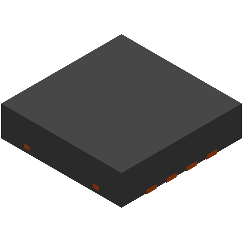
3D Model
Available Download Formats
By downloading CAD models, you agree to our Terms & Conditions and Privacy Policy

1.5-Gbps differential buffer with adjustable output voltage 8-WSON -40 to 85
Tip: Data for a part may vary between manufacturers. You can filter for manufacturers on the top of the page next to the part image and part number.
| Part # | Distributor | Description | Stock | Price | Buy | |
|---|---|---|---|---|---|---|
|
DISTI #
DS15BA101SDE/NOPBCT-ND
|
DigiKey | IC REDRIVER LVDS 1CH 8WSON Min Qty: 1 Lead time: 6 Weeks Container: Cut Tape (CT), Digi-Reel®, Tape & Reel (TR) |
268 In Stock |
|
$2.6947 / $5.3700 | Buy Now |
|
DISTI #
926-DS15BA101SDENOPB
|
Mouser Electronics | Buffers & Line Drivers 1.5Gbps Diff Buffer w/ Adj Output Vtg RoHS: Compliant | 746 |
|
$2.6700 / $5.2100 | Buy Now |
|
|
Rochester Electronics | DS15BA101 1.5-Gbps differential buffer with adjustable output voltage RoHS: Compliant Status: Active Min Qty: 1 | 5834 |
|
$2.4900 / $2.9300 | Buy Now |
|
|
Ameya Holding Limited | DS15BA101SDE/NOPB , 2Gbit/s LVDS 缓冲器, CML/ LVDS/ LVPECL输入, 8针 LLP封装 | 93007 |
|
RFQ |
By downloading CAD models, you agree to our Terms & Conditions and Privacy Policy
|
|
DS15BA101SDE/NOPB
Texas Instruments
Buy Now
Datasheet
|
Compare Parts:
DS15BA101SDE/NOPB
Texas Instruments
1.5-Gbps differential buffer with adjustable output voltage 8-WSON -40 to 85
|
| Pbfree Code | Yes | |
| Rohs Code | Yes | |
| Part Life Cycle Code | Active | |
| Ihs Manufacturer | TEXAS INSTRUMENTS INC | |
| Part Package Code | SON | |
| Package Description | WSON-8 | |
| Pin Count | 8 | |
| Reach Compliance Code | compliant | |
| ECCN Code | EAR99 | |
| HTS Code | 8542.39.00.01 | |
| Samacsys Manufacturer | Texas Instruments | |
| Amplifier Type | BUFFER | |
| JESD-30 Code | S-PDSO-N8 | |
| JESD-609 Code | e3 | |
| Length | 3 mm | |
| Moisture Sensitivity Level | 3 | |
| Number of Functions | 1 | |
| Number of Terminals | 8 | |
| Operating Temperature-Max | 85 °C | |
| Operating Temperature-Min | -40 °C | |
| Package Body Material | PLASTIC/EPOXY | |
| Package Code | HVSON | |
| Package Shape | SQUARE | |
| Package Style | SMALL OUTLINE, HEAT SINK/SLUG, VERY THIN PROFILE | |
| Packing Method | TR | |
| Peak Reflow Temperature (Cel) | 260 | |
| Seated Height-Max | 0.8 mm | |
| Supply Current-Max | 49 mA | |
| Supply Voltage Limit-Max | 3.6 V | |
| Supply Voltage-Nom (Vsup) | 3.3 V | |
| Surface Mount | YES | |
| Temperature Grade | INDUSTRIAL | |
| Terminal Finish | MATTE TIN | |
| Terminal Form | NO LEAD | |
| Terminal Pitch | 0.5 mm | |
| Terminal Position | DUAL | |
| Time@Peak Reflow Temperature-Max (s) | 30 | |
| Width | 3 mm |
This table gives cross-reference parts and alternative options found for DS15BA101SDE/NOPB. The Form Fit Function (FFF) tab will give you the options that are more likely to serve as direct pin-to-pin alternates or drop-in parts. The Functional Equivalents tab will give you options that are likely to match the same function of DS15BA101SDE/NOPB, but it may not fit your design. Always verify details of parts you are evaluating, as these parts are offered as suggestions for what you are looking for and are not guaranteed.
| Part Number | Description | Manufacturer | Compare |
|---|---|---|---|
| DS15BA101SDX/NOPB | 1.5-Gbps differential buffer with adjustable output voltage 8-WSON -40 to 85 | Texas Instruments | DS15BA101SDE/NOPB vs DS15BA101SDX/NOPB |
| DS15BA101SD/NOPB | 1.5-Gbps differential buffer with adjustable output voltage 8-WSON -40 to 85 | Texas Instruments | DS15BA101SDE/NOPB vs DS15BA101SD/NOPB |
| DS15BA101SD | BUFFER AMPLIFIER, DSO8, 3 X 3 MM, LLP-8 | Texas Instruments | DS15BA101SDE/NOPB vs DS15BA101SD |