Note: Data for a part may vary between manufacturers. You can filter for manufacturers on the top of the page next to the part image and part number.
6 listings
)
1 cross
)
Available
)
1 cross
)
Available
)
Where used in Applications:
Consumer Electronics
Energy and Power Systems
Transportation and Logistics
Renewable Energy
Automotive
Part #
Manufacturer
Description
Stock
Price
Buy
Details
DigiKey
IC REG BOOST ADJ 350MA 12WSON
Min Qty:
1
Lead time:
18 Weeks
Container:
Digi-Reel®, Cut Tape (CT), Tape & Reel (TR)
10437
1
$1.5500
10
$1.3820
25
$1.3120
100
$1.0779
250
$1.0076
500
$0.8904
1,000
$0.7030
3,000
$0.6561
6,000
$0.6233
15,000
$0.5999
$0.5999 / $1.5500
Buy Now
Details
DISTI #
595-TPS61096ADSSR
Mouser Electronics
Switching Voltage Regulators 28-V Output Voltage Boost Converter with 1-uA Quiescent Current 12-WSON -40 to 125
RoHS:
Compliant
8033
1
$1.5500
10
$1.3200
100
$1.0100
500
$0.8900
1,000
$0.7030
3,000
$0.6060
6,000
$0.5860
9,000
$0.5850
$0.5850 / $1.5500
Buy Now
Details
Ameya Holding Limited
220286
RFQ
Details
LCSC
USON-12-EP(2x3) DC-DC Converters ROHS
98
1
$1.4447
10
$1.2471
30
$1.1237
100
$0.9971
500
$0.9400
1,000
$0.9153
$0.9153 / $1.4447
Buy Now
Details
Vyrian
OEM/CM Only
200
RFQ
Details
Win Source Electronics
IC REG BOOST ADJ 350MA 12WSON
208100
60
$0.8480
145
$0.6960
225
$0.6740
310
$0.6530
400
$0.6310
535
$0.5660
$0.5660 / $0.8480
Buy Now
Part Symbol
Footprint
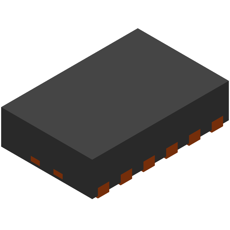
3D Model
ADJUSTABLE OUTPUT VOLTAGE FROM 4.5 V TO 28 V
PULSE FREQUENCY MODULATION
Moisture Sensitivity Level
Operating Temperature-Max
Operating Temperature-Min
SMALL OUTLINE, HEAT SINK/SLUG, VERY THIN PROFILE
Peak Reflow Temperature (Cel)
Time@Peak Reflow Temperature-Max (s)
Want to compare parts?
Texas Instruments
28-V Output Voltage Boost Converter with 1-µA Quiescent Current 12-WSON -40 to 125
VS
Select a part to compare
Choose Part to Compare
Search a specific part
TPS61096ADSST - Texas Instruments
TPS61096ADSST - Texas Instruments
This table gives cross-reference parts and alternative options found for TPS61096ADSSR. The Form Fit Function (FFF) tab will give you the options that are more likely to serve as direct pin-to-pin alternates or drop-in parts. The Functional Equivalents tab will give you options that are likely to match the same function of TPS61096ADSSR, but it may not fit your design. Always verify details of parts you are evaluating, as these parts are offered as suggestions for what you are looking for and are not guaranteed.
Part Number
Description
Manufacturer
Compare
TPS61096ADSST
28-V Output Voltage Boost Converter with 1-µA Quiescent Current 12-WSON -40 to 125
Texas Instruments
TPS61096ADSSR vs TPS61096ADSST
Part Number
Description
Manufacturer
Compare
TPS61096ADSST
28-V Output Voltage Boost Converter with 1-µA Quiescent Current 12-WSON -40 to 125
Texas Instruments
TPS61096ADSSR vs TPS61096ADSST