Tip: Data for a part may vary between manufacturers. You can filter for manufacturers on the top of the page next to the part image and part number.
ApplicationsEducation and ResearchIndustrial AutomationFinancial Technology (Fintech)HealthcareElectronic Manufacturing
CD4512BF Information
CD4512BF by Texas Instruments is a Multiplexer/Demultiplexer.
Multiplexer/Demultiplexers are under the broader part category of Logic Components.
Digital logic governs the behavior of signals in electronic circuits, enabling complex decisions based on simple binary inputs (yes/no). Logic components perform operations from these signals. Read more about Logic Components on our Logic part category page.
US Tariff Estimator: CD4512BF by Texas Instruments
Calculations from this tool are estimations only for imports into the United States. Please refer to the distributor or manufacturer and reference official US government sources and authorities to verify any final purchase costs.
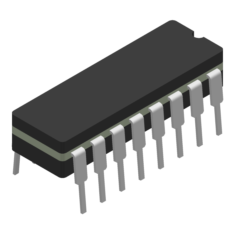
CD4512BFTexas InstrumentsMultiplexer, 4000/14000/40000 Series, 1-Func, 8 Line Input, 1 Line Output, True Output, CMOS, CDIP16
Pbfree Code
Yes
Part Life Cycle Code
Active
Part Package Code
DIP
Pin Count
16
ECCN Code
EAR99
HTS Code
8542.39.00.90
Family
4000/14000/40000
JESD-30 Code
R-GDIP-T16
JESD-609 Code
e0
Length
19.56 Mm
Load Capacitance (CL)
50 Pf
Logic IC Type
Multiplexer
Max I(ol)
0.0015 A
Number of Bits
8
Number of Functions
1
Number of Inputs
8
Number of Outputs
1
Number of Terminals
16
Operating Temperature-Max
125 °C
Operating Temperature-Min
-55 °C
Output Characteristics
3-State
Output Polarity
True
Package Body Material
Ceramic, Glass-Sealed
Package Code
DIP
Package Equivalence Code
DIP16,.3
Package Shape
Rectangular
Package Style
In-Line
Packing Method
Tube
Power Supply Current-Max (ICC)
3 Ma
Prop. Delay@Nom-Sup
140 Ns
Propagation Delay (tpd)
360 Ns
Qualification Status
Not Qualified
Seated Height-Max
5.08 Mm
Supply Voltage-Max (Vsup)
18 V
Supply Voltage-Min (Vsup)
3 V
Supply Voltage-Nom (Vsup)
5 V
Surface Mount
No
Technology
Cmos
Temperature Grade
Military
Terminal Finish
Tin/Lead (Sn/Pb)
Terminal Form
Through-Hole
Terminal Pitch
2.54 Mm
Terminal Position
Dual
Width
7.62 Mm
Alternate Parts for CD4512BF
This table gives cross-reference parts and alternative options found for CD4512BF. The Form Fit Function (FFF) tab will give you the options that are more likely to serve as direct pin-to-pin alternates or drop-in parts. The Functional Equivalents tab will give you options that are likely to match the same function of CD4512BF, but it may not fit your design. Always verify details of parts you are evaluating, as these parts are offered as suggestions for what you are looking for and are not guaranteed.
The CD4512BF can handle clock frequencies up to 10 MHz, but it's recommended to limit it to 5 MHz for reliable operation.
To ensure proper reset, connect the RST pin to VCC through a 1kΩ resistor and a 10nF capacitor to ground. This will provide a clean reset signal during power-up.
The recommended operating voltage range for the CD4512BF is 4.5V to 5.5V, with a typical operating voltage of 5V.
The CD4512BF can be interfaced with a microcontroller using a 4-bit or 8-bit bus. Connect the CD4512BF's data pins (D0-D3 or D0-D7) to the microcontroller's data bus, and the CD4512BF's control pins (RST, CE, and CLK) to the microcontroller's control signals.
The CE pin is used to enable or disable the CD4512BF. When CE is low, the device is enabled and responds to clock and data inputs. When CE is high, the device is disabled and ignores clock and data inputs.