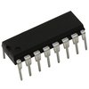
Part Details for L2720 by STMicroelectronics
Results Overview of L2720 by STMicroelectronics
- Distributor Offerings: (2 listings)
- Number of FFF Equivalents: (0 replacements)
- Tariff Estimator: (Available) NEW
- Number of Functional Equivalents: (0 options)
- CAD Models: (Request Part)
- Part Data Attributes: (Available)
- Reference Designs: (Not Available)
Tip: Data for a part may vary between manufacturers. You can filter for manufacturers on the top of the page next to the part image and part number.
L2720 Information
L2720 by STMicroelectronics is an Operational Amplifier.
Operational Amplifiers are under the broader part category of Amplifier Circuits.
Amplifier circuits use external power to increase the amplitude of an input signal. They can be used to perform linear amplifications or logarithmic functions. Read more about Amplifier Circuits on our Amplifier Circuits part category page.
Price & Stock for L2720
| Part # | Distributor | Description | Stock | Price | Buy | |
|---|---|---|---|---|---|---|
|
DISTI #
NS-L2720
|
Northstar Micro Electronics | OEM/CM ONLY | 8776 |
|
Buy Now RFQ | |
|
|
Vyrian | Operational Amplifier, 2 Func, 10000uV Offset-Max, BIPolar, PDIP16 | 4933 |
|
RFQ |
US Tariff Estimator: L2720 by STMicroelectronics
Calculations from this tool are estimations only for imports into the United States. Please refer to the distributor or manufacturer and reference official US government sources and authorities to verify any final purchase costs.
L2720 Part Data Attributes
|
|
L2720
STMicroelectronics
Buy Now
Datasheet
|
Compare Parts:
L2720
STMicroelectronics
Operational Amplifier, 16 Func, 10000uV Offset-Max, BIPolar, PDIP2
|
| Pbfree Code | Yes | |
| Rohs Code | Yes | |
| Part Life Cycle Code | Obsolete | |
| Part Package Code | DIP | |
| Package Description | Power, Dip-16 | |
| Pin Count | 16 | |
| ECCN Code | EAR99 | |
| HTS Code | 8542.33.00.01 | |
| Amplifier Type | Operational Amplifier | |
| Architecture | Voltage-Feedback | |
| Average Bias Current-Max (IIB) | 1 µA | |
| Bias Current-Max (IIB) @25C | 1 µA | |
| Common-mode Reject Ratio-Min | 66 Db | |
| Common-mode Reject Ratio-Nom | 84 Db | |
| Frequency Compensation | Yes | |
| Input Offset Voltage-Max | 10000 µV | |
| JESD-30 Code | R-PDIP-T16 | |
| JESD-609 Code | e3 | |
| Length | 20 Mm | |
| Low-Bias | No | |
| Low-Offset | No | |
| Micropower | No | |
| Number of Functions | 16 | |
| Number of Terminals | 2 | |
| Operating Temperature-Max | 85 °C | |
| Operating Temperature-Min | -40 °C | |
| Package Body Material | Plastic/Epoxy | |
| Package Code | DIP | |
| Package Equivalence Code | DIP16,.4 | |
| Package Shape | Rectangular | |
| Package Style | In-Line | |
| Packing Method | No | |
| Power | Yes | |
| Programmable Power | No | |
| Qualification Status | Not Qualified | |
| Seated Height-Max | 5.1 Mm | |
| Slew Rate-Nom | 2 V/Us | |
| Supply Current-Max | 15 Ma | |
| Supply Voltage Limit-Max | 28 V | |
| Supply Voltage-Nom (Vsup) | 24 V | |
| Surface Mount | No | |
| Technology | Bipolar | |
| Temperature Grade | Industrial | |
| Terminal Finish | Matte Tin | |
| Terminal Form | Through-Hole | |
| Terminal Pitch | 2.54 Mm | |
| Terminal Position | Dual | |
| Unity Gain BW-Nom | 1200 | |
| Voltage Gain-Min | 3160 | |
| Wideband | No | |
| Width | 7.62 Mm |
L2720 Frequently Asked Questions (FAQ)
-
The maximum output current of the L2720 is 3A per channel, but it's recommended to limit it to 2A per channel for reliable operation and to prevent overheating.
-
To ensure the L2720 operates within its SOA, you should monitor the junction temperature, output current, and input voltage. Make sure to keep the junction temperature below 150°C, output current below 2A per channel, and input voltage within the recommended range.
-
The bootstrap capacitor (CB) is used to generate the high-side gate drive voltage for the internal power MOSFETs. It's essential to choose a capacitor with a high voltage rating and low ESR to ensure proper operation.
-
The minimum input capacitance (CIN) can be calculated using the formula: CIN = (IOUT x VOUT) / (fSW x ΔV). Where IOUT is the output current, VOUT is the output voltage, fSW is the switching frequency, and ΔV is the input voltage ripple.
-
For optimal performance and thermal management, it's recommended to follow a 4-layer PCB design with a dedicated ground plane, keep the input and output capacitors close to the IC, and use a thermal pad or heat sink for the L2720.