-
Part Symbol
-
Footprint
-
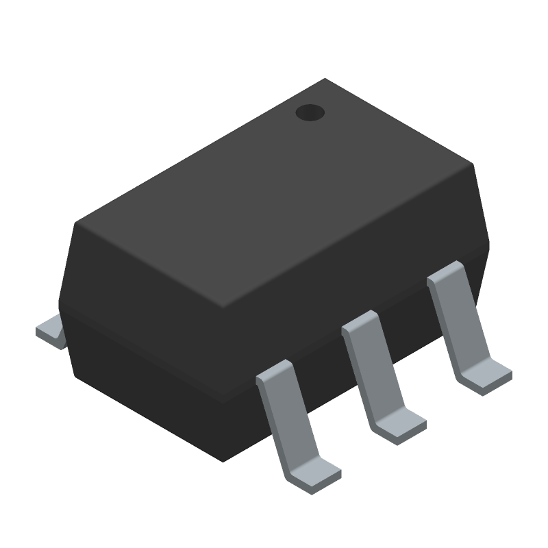
3D Model
Available Download Formats
By downloading CAD models, you agree to our Terms & Conditions and Privacy Policy
100MHz - 3000MHz RF/MICROWAVE WIDE BAND LOW POWER AMPLIFIER, MINIATURE, SC-70, SOT-363, 6 PIN
Tip: Data for a part may vary between manufacturers. You can filter for manufacturers on the top of the page next to the part image and part number.
MGA-62563-TR1G by Avago Technologies is an RF/Microwave Amplifier.
RF/Microwave Amplifiers are under the broader part category of RF and Microwave Components.
RF and Microwave Engineering focuses on the design and operation of devices that transmit or receive radio waves. The main distinction between RF and microwave engineering is their wavelength, which influences how energy is transmitted and used in various applications. Read more about RF and Microwave Components on our RF and Microwave part category page.
| Part # | Manufacturer | Description | Datasheet |
|---|---|---|---|
| UC2827DWTR-1G4 | Texas Instruments | Buck Current/Voltage Fed Push-Pull PWM Controllers 24-SOIC -40 to 85 | |
| UCC2808ADTR-1G4 | Texas Instruments | Low-Power Current-Mode Push-Pull PWM 8-SOIC -40 to 85 | |
| UCC2809PTR-1G4 | Texas Instruments | Economy Primary Side Controller 8-VSSOP -40 to 85 |
| Part # | Distributor | Description | Stock | Price | Buy | |
|---|---|---|---|---|---|---|
|
|
Bristol Electronics | 180 |
|
RFQ | ||
|
|
Chip Stock | ICRfAmp100MHZ-3GHZSOT363", rfAmplifierIC100MHZ~3GHZSOT-363,SC70", | 29090 |
|
RFQ |
By downloading CAD models, you agree to our Terms & Conditions and Privacy Policy
|
|
MGA-62563-TR1G
Avago Technologies
Buy Now
Datasheet
|
Compare Parts:
MGA-62563-TR1G
Avago Technologies
100MHz - 3000MHz RF/MICROWAVE WIDE BAND LOW POWER AMPLIFIER, MINIATURE, SC-70, SOT-363, 6 PIN
|
| Pbfree Code | Yes | |
| Rohs Code | Yes | |
| Part Life Cycle Code | Obsolete | |
| Package Description | Tssop6,.08 | |
| Reach Compliance Code | Compliant | |
| Characteristic Impedance | 50 Ω | |
| Construction | Component | |
| Gain | 20.4 Db | |
| Input Power-Max (CW) | 21 Dbm | |
| JESD-609 Code | e3 | |
| Mounting Feature | Surface Mount | |
| Number of Functions | 1 | |
| Number of Terminals | 6 | |
| Operating Frequency-Max | 3000 Mhz | |
| Operating Frequency-Min | 100 Mhz | |
| Package Body Material | Plastic/Epoxy | |
| Package Equivalence Code | TSSOP6,.08 | |
| Power Supplies | 3/5 V | |
| RF/Microwave Device Type | Wide Band Low Power | |
| Supply Current-Max | 77 Ma | |
| Surface Mount | Yes | |
| Technology | Gaas | |
| Terminal Finish | Tin (Sn) | |
| VSWR-Max | 2 |
This table gives cross-reference parts and alternative options found for MGA-62563-TR1G. The Form Fit Function (FFF) tab will give you the options that are more likely to serve as direct pin-to-pin alternates or drop-in parts. The Functional Equivalents tab will give you options that are likely to match the same function of MGA-62563-TR1G, but it may not fit your design. Always verify details of parts you are evaluating, as these parts are offered as suggestions for what you are looking for and are not guaranteed.
| Part Number | Manufacturer | Composite Price | Description | Compare |
|---|---|---|---|---|
| MGA-62563-TR1 | Agilent Technologies Inc | Check for Price | Wide Band Low Power Amplifier, 100MHz Min, 3000MHz Max, 1 Func, GAAS, SOT-363, 6 PIN | MGA-62563-TR1G vs MGA-62563-TR1 |
| MGA-62563-TR2G | Agilent Technologies Inc | Check for Price | Wide Band Low Power Amplifier, 100MHz Min, 3000MHz Max, 1 Func, GAAS, SOT-363, 6 PIN | MGA-62563-TR1G vs MGA-62563-TR2G |
| MGA-62563-BLK | Agilent Technologies Inc | Check for Price | Wide Band Low Power Amplifier, 100MHz Min, 3000MHz Max, 1 Func, GAAS, SOT-363, 6 PIN | MGA-62563-TR1G vs MGA-62563-BLK |
| MGA-62563-TR2 | Agilent Technologies Inc | Check for Price | Wide Band Low Power Amplifier, 100MHz Min, 3000MHz Max, 1 Func, GAAS, SOT-363, 6 PIN | MGA-62563-TR1G vs MGA-62563-TR2 |
A 4-layer PCB with a solid ground plane and thermal vias is recommended. Ensure a minimum of 1mm clearance around the device for heat dissipation. A thermal pad on the bottom of the package should be connected to a solid ground plane.
Use a 50-ohm transmission line, keep signal traces short and away from noise sources, and use shielding or guard traces to minimize EMI. Also, ensure that the device is properly decoupled with 0.1uF and 10uF capacitors.
Power up the device in the following sequence: VCC, AVDD, DVDD, and finally, the input signals. The voltage ramp rate should be 1-2mV/us to prevent latch-up and ensure reliable operation.
Use a logic analyzer or oscilloscope to capture waveforms and verify signal integrity. Check the device's output for correct voltage levels and signal timing. Consult the datasheet and application notes for troubleshooting guides and FAQs.
The device is rated for operation from -40°C to 85°C. Ensure that the device is stored and operated within these temperature limits. Follow the recommended soldering and handling procedures to prevent damage and ensure reliability.