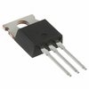
| Part Number | Manufacturer | Composite Price | Description | Compare |
|---|---|---|---|---|
| PIP3115-B,118 | NXP Semiconductors | Check for Price | Buffer/Inverter Based Peripheral Driver, PSSO2 | VNP5N07 vs PIP3115-B,118 |
| BTS117BKSA1 | Infineon Technologies AG | Check for Price | Fixed, 1 Channel, PSFM3 | VNP5N07 vs BTS117BKSA1 |
| 934056824118 | NXP Semiconductors | Check for Price | Buffer/Inverter Based Peripheral Driver, 12A, PSSO2 | VNP5N07 vs 934056824118 |
Part Details for VNP5N07 by STMicroelectronics
Results Overview of VNP5N07 by STMicroelectronics
- Distributor Offerings: (3 listings)
- Number of FFF Equivalents: (0 replacements)
- Tariff Estimator: (Available) NEW
- Number of Functional Equivalents: (3 options)
- CAD Models: (Available)
- Part Data Attributes: (Available)
- Reference Designs: (Not Available)
Tip: Data for a part may vary between manufacturers. You can filter for manufacturers on the top of the page next to the part image and part number.
Applications
Energy and Power Systems
Renewable Energy
VNP5N07 Information
VNP5N07 by STMicroelectronics is a Peripheral Driver.
Peripheral Drivers are under the broader part category of Drivers And Interfaces.
A driver controls the current or voltage delivered to components like LCDs or motors, while an interface component connects systems for data transfer and control. Read more about Drivers And Interfaces on our Drivers And Interfaces part category page.
Price & Stock for VNP5N07
| Part # | Distributor | Description | Stock | Price | Buy | |
|---|---|---|---|---|---|---|
|
|
ComSIT USA | OMNIFET FULLY AUTOPROTECTED POWER MOSFET Buffer/Inverter Based Peripheral Driver, 5A, MOS, PSFM3 ECCN: EAR99 RoHS: Compliant |
|
|
RFQ | |
|
|
Chip Stock | Power Switch Lo Side 5A 3-Pin(3+Tab) TO-220 Tube | 10507 |
|
RFQ | |
|
|
Vyrian | Buffer/Inverter Based Peripheral Driver, 5A, MOS, PSFM3 | 7664 |
|
RFQ |
US Tariff Estimator: VNP5N07 by STMicroelectronics
Calculations from this tool are estimations only for imports into the United States. Please refer to the distributor or manufacturer and reference official US government sources and authorities to verify any final purchase costs.
VNP5N07 CAD Models
-
Part Symbol
-
Footprint
Available Download Formats
By downloading CAD models, you agree to our Terms & Conditions and Privacy Policy
VNP5N07 Part Data Attributes
|
|
VNP5N07
STMicroelectronics
Buy Now
Datasheet
|
Compare Parts:
VNP5N07
STMicroelectronics
Buffer/Inverter Based Peripheral Driver, 5A, MOS, PSFM3
|
| Rohs Code | Yes | |
| Part Life Cycle Code | Obsolete | |
| Part Package Code | SFM | |
| Package Description | To-220, 3 Pin | |
| Pin Count | 3 | |
| ECCN Code | EAR99 | |
| HTS Code | 8542.39.00.60 | |
| Built-in Protections | Transient; Over Current; Over Voltage; Thermal | |
| Input Characteristics | Schmitt Trigger | |
| Interface IC Type | Buffer Or Inverter Based Peripheral Driver | |
| JESD-30 Code | R-PSFM-T3 | |
| JESD-609 Code | e3 | |
| Number of Functions | 1 | |
| Number of Terminals | 3 | |
| Output Characteristics | Open-Drain | |
| Output Current Flow Direction | Sink | |
| Output Peak Current Limit-Nom | 5 A | |
| Output Polarity | True | |
| Package Body Material | Plastic/Epoxy | |
| Package Code | SFM | |
| Package Shape | Rectangular | |
| Package Style | Flange Mount | |
| Qualification Status | Not Qualified | |
| Supply Current-Max | 0.5 Ma | |
| Surface Mount | No | |
| Technology | Mos | |
| Terminal Finish | Matte Tin (Sn) | |
| Terminal Form | Through-Hole | |
| Terminal Position | Single | |
| Turn-off Time | 5 µS | |
| Turn-on Time | 0.25 µS |
Alternate Parts for VNP5N07
This table gives cross-reference parts and alternative options found for VNP5N07. The Form Fit Function (FFF) tab will give you the options that are more likely to serve as direct pin-to-pin alternates or drop-in parts. The Functional Equivalents tab will give you options that are likely to match the same function of VNP5N07, but it may not fit your design. Always verify details of parts you are evaluating, as these parts are offered as suggestions for what you are looking for and are not guaranteed.
VNP5N07 Frequently Asked Questions (FAQ)
-
The maximum operating temperature range for the VNP5N07 is -40°C to 150°C.
-
To ensure proper biasing, connect VCC to a stable 5V power supply, and connect VEE to a stable -5V power supply. Also, ensure that the input voltage (VIN) is within the recommended range of 4.5V to 5.5V.
-
To minimize noise and EMI, use a multi-layer PCB with a solid ground plane, and keep the input and output traces as short as possible. Also, use a decoupling capacitor (e.g., 100nF) between VCC and GND, and another between VIN and GND.
-
To protect the VNP5N07 from overvoltage and overcurrent, use a voltage regulator (e.g., 5V) to regulate the input voltage, and add a current-limiting resistor (e.g., 1kΩ) in series with the input voltage. Also, consider adding a TVS (Transient Voltage Suppressor) diode to protect against voltage spikes.
-
The recommended input capacitance for the VNP5N07 is 100nF to 1μF, depending on the specific application and noise requirements.