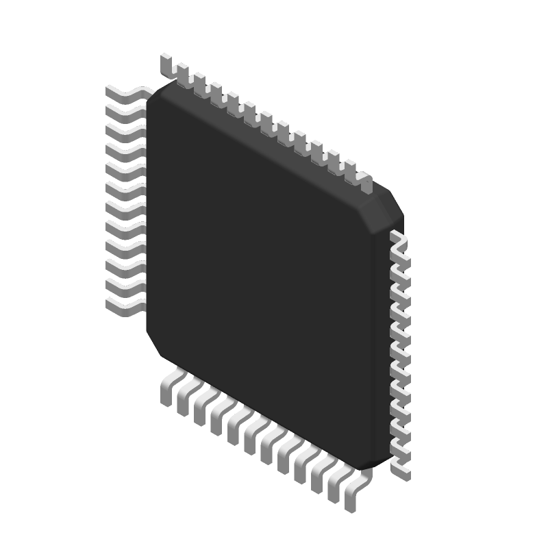
Tip: Data for a part may vary between manufacturers. You can filter for manufacturers on the top of the page next to the part image and part number.
ApplicationsEducation and ResearchInternet of Things (IoT)Industrial AutomationComputing and Data StorageAerospace and DefenseHealthcareTelecommunicationsElectronic ManufacturingAutomotive
ADS8412IPFBT Information
ADS8412IPFBT by Texas Instruments is an Analog to Digital Converter.
Analog to Digital Converters are under the broader part category of Converters.
A converter is an electrical circuit that transforms electric energy into a different form that will support a elecrical load needed by a device. Read more about Converters on our Converters part category page.
US Tariff Estimator: ADS8412IPFBT by Texas Instruments
Calculations from this tool are estimations only for imports into the United States. Please refer to the distributor or manufacturer and reference official US government sources and authorities to verify any final purchase costs.
This table gives cross-reference parts and alternative options found for ADS8412IPFBT. The Form Fit Function (FFF) tab will give you the options that are more likely to serve as direct pin-to-pin alternates or drop-in parts. The Functional Equivalents tab will give you options that are likely to match the same function of ADS8412IPFBT, but it may not fit your design. Always verify details of parts you are evaluating, as these parts are offered as suggestions for what you are looking for and are not guaranteed.
Texas Instruments provides a layout guide in the datasheet, but it's also recommended to follow general high-speed PCB design guidelines, such as using a solid ground plane, minimizing trace lengths, and using differential pairs for clock and data signals.
The clock input should be driven differentially, and the signal should be terminated with a 100-ohm resistor to match the impedance of the clock input. Additionally, the clock signal should be filtered to remove high-frequency noise.
The recommended power-up sequence is to power up the analog supply (AVDD) first, followed by the digital supply (DVDD), and then the clock signal. This ensures that the analog circuitry is stable before the digital circuitry is enabled.
To optimize performance in a noisy environment, use shielding, filtering, and decoupling to reduce electromagnetic interference (EMI). Additionally, use a low-noise power supply, and consider using a ferrite bead or common-mode choke to filter the clock signal.
The maximum clock frequency is 65 MSPS, but this can be limited by the specific application and the quality of the clock signal. It's recommended to consult the datasheet and application notes for specific guidance on clock frequency selection.