-
3D Model
Available Download Formats
By downloading CAD models, you agree to our Terms & Conditions and Privacy Policy

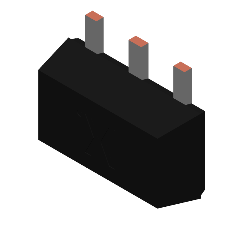
BSS192 - 240 V, P-channel vertical D-MOS transistor@en-us SOT-89 3-Pin
Tip: Data for a part may vary between manufacturers. You can filter for manufacturers on the top of the page next to the part image and part number.
BSS192,135 by Nexperia is a Small Signal Field-Effect Transistor.
Small Signal Field-Effect Transistors are under the broader part category of Transistors.
A transistor is a small semiconductor device used to amplify, control, or create electrical signals. When selecting a transistor, factors such as voltage, current rating, gain, and power dissipation must be considered, with common types. Read more about Transistors on our Transistors part category page.
| Part # | Distributor | Description | Stock | Price | Buy | |
|---|---|---|---|---|---|---|
|
DISTI #
BSS192,135-ND
|
DigiKey | MOSFET P-CH 240V 200MA SOT89 Min Qty: 20000 Lead time: 26 Weeks Container: Tape & Reel (TR) | Limited Supply - Call |
|
$0.1803 | Buy Now |
|
DISTI #
BSS192,135
|
Avnet Americas | Trans MOSFET P-CH 240V 0.2A 4-Pin(3+Tab) SOT-89 T/R - Tape and Reel (Alt: BSS192,135) COO: China RoHS: Compliant Min Qty: 20000 Package Multiple: 4000 Lead time: 53 Weeks, 1 Days Container: Tape & Reel | 0 |
|
$0.1731 / $0.2007 | Buy Now |
|
DISTI #
771-BSS192135
|
Mouser Electronics | MOSFETs BSS192/SOT89/MPT3 RoHS: Compliant | 0 |
|
Order Now | |
|
|
Chip Stock | TransMOSFETP-CH240V0.2A4-Pin(3+Tab)SOT-89T/R | 126000 |
|
RFQ | |
|
|
Vyrian | Other Function Semiconductors | 4037 |
|
RFQ |
By downloading CAD models, you agree to our Terms & Conditions and Privacy Policy
|
|
BSS192,135
Nexperia
Buy Now
Datasheet
|
Compare Parts:
BSS192,135
Nexperia
BSS192 - 240 V, P-channel vertical D-MOS transistor@en-us SOT-89 3-Pin
|
| Rohs Code | Yes | |
| Part Life Cycle Code | Not Recommended | |
| Part Package Code | SOT-89 | |
| Package Description | Sc-62, To-243, 3 Pin | |
| Pin Count | 3 | |
| Manufacturer Package Code | SOT89 | |
| Reach Compliance Code | Compliant | |
| ECCN Code | EAR99 | |
| Factory Lead Time | 8 Weeks | |
| Case Connection | Drain | |
| Configuration | Single With Built-In Diode | |
| DS Breakdown Voltage-Min | 240 V | |
| Drain Current-Max (ID) | 0.2 A | |
| Drain-source On Resistance-Max | 12 Ω | |
| FET Technology | Metal-Oxide Semiconductor | |
| Feedback Cap-Max (Crss) | 15 Pf | |
| JEDEC-95 Code | TO-243AA | |
| JESD-30 Code | R-PSSO-F3 | |
| JESD-609 Code | e3 | |
| Moisture Sensitivity Level | 1 | |
| Number of Elements | 1 | |
| Number of Terminals | 3 | |
| Operating Mode | Enhancement Mode | |
| Package Body Material | Plastic/Epoxy | |
| Package Shape | Rectangular | |
| Package Style | Small Outline | |
| Peak Reflow Temperature (Cel) | 260 | |
| Polarity/Channel Type | P-Channel | |
| Reference Standard | Iec-60134 | |
| Surface Mount | Yes | |
| Terminal Finish | Tin | |
| Terminal Form | Flat | |
| Terminal Position | Single | |
| Time@Peak Reflow Temperature-Max (s) | 30 | |
| Transistor Application | Switching | |
| Transistor Element Material | Silicon |
This table gives cross-reference parts and alternative options found for BSS192,135. The Form Fit Function (FFF) tab will give you the options that are more likely to serve as direct pin-to-pin alternates or drop-in parts. The Functional Equivalents tab will give you options that are likely to match the same function of BSS192,135, but it may not fit your design. Always verify details of parts you are evaluating, as these parts are offered as suggestions for what you are looking for and are not guaranteed.
| Part Number | Manufacturer | Composite Price | Description | Compare |
|---|---|---|---|---|
| BSS192,115 | Nexperia | $0.5931 | BSS192 - 240 V, P-channel vertical D-MOS transistor@en-us SOT-89 3-Pin | BSS192,135 vs BSS192,115 |
| 933943950135 | Nexperia | Check for Price | Small Signal Field-Effect Transistor, 0.2A I(D), 240V, 1-Element, P-Channel, Silicon, Metal-oxide Semiconductor FET, TO-243AA | BSS192,135 vs 933943950135 |
| BSS192 | Nexperia | Check for Price | Small Signal Field-Effect Transistor, 0.2A I(D), 240V, 1-Element, P-Channel, Silicon, Metal-oxide Semiconductor FET, TO-243AA | BSS192,135 vs BSS192 |
The maximum operating temperature range for the BSS192,135 is -55°C to 150°C, but it's recommended to operate within -40°C to 125°C for optimal performance and reliability.
To ensure proper biasing, make sure to provide a stable voltage supply, keep the input voltage within the recommended range (VCC = 2.7 V to 5.5 V), and maintain a low impedance output load. Additionally, ensure the device is properly decoupled with capacitors to minimize noise and oscillations.
For optimal thermal management, use a multi-layer PCB with a solid ground plane, and place the device near a heat sink or a thermal pad. Ensure good thermal conductivity by using thermal vias and a sufficient copper area. Keep the device away from high-current paths and noisy signals to minimize electromagnetic interference (EMI).
To prevent electrostatic discharge (ESD) damage, handle the device by the body or use an anti-static wrist strap. Ensure the PCB is designed with ESD protection in mind, using components like TVS diodes or ESD protection arrays. Follow proper assembly and handling procedures to minimize the risk of ESD damage.
When using the BSS192,135 in a high-frequency application, consider the device's frequency response, parasitic capacitance, and inductance. Ensure the PCB layout is optimized for high-frequency operation, using techniques like impedance matching, shielding, and minimizing trace lengths. Additionally, consider using a device with a higher frequency rating or a dedicated high-frequency transistor.