
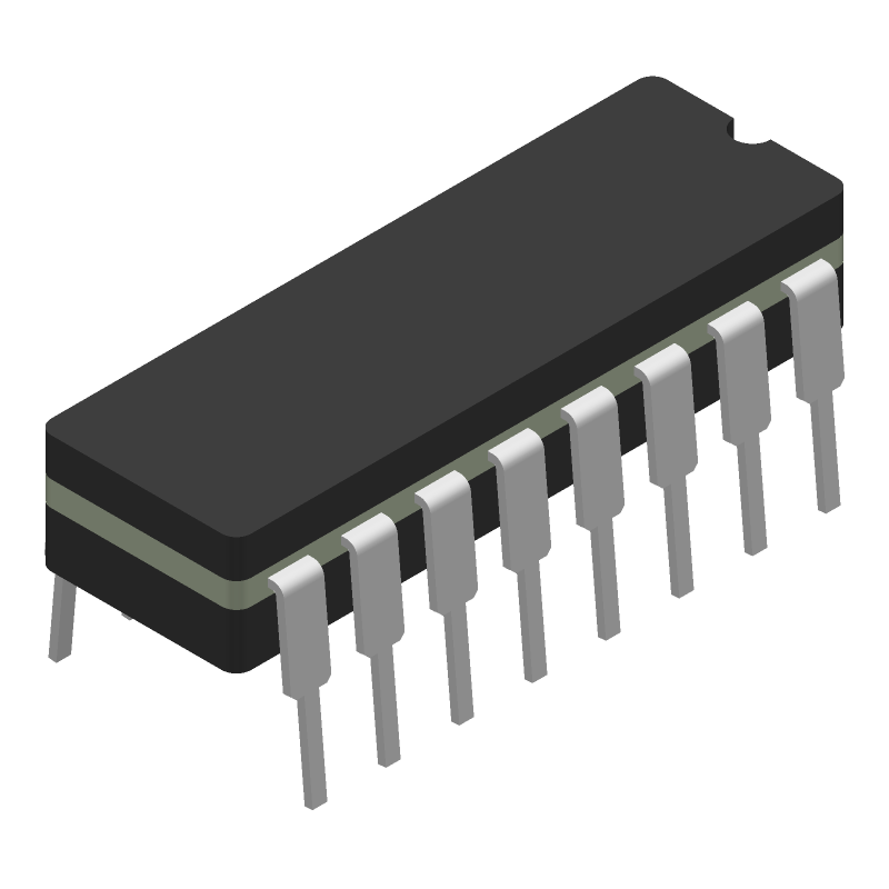
| Part Number | Manufacturer | Composite Price | Description | Compare |
|---|---|---|---|---|
| MC74HC4052ANG | onsemi | Check for Price | Differential Multiplexer, 1 Func, 4 Channel, CMOS, PDIP16 | CD54HC4052F3A vs MC74HC4052ANG |
| 74HC4052N,652 | NXP Semiconductors | Check for Price | Differential Multiplexer, 1 Func, 4 Channel, CMOS, PDIP16 | CD54HC4052F3A vs 74HC4052N,652 |
| CD74HC4052E | Harris Semiconductor | Check for Price | Differential Multiplexer, 1 Func, 4 Channel, CMOS, PDIP16 | CD54HC4052F3A vs CD74HC4052E |
| HD74HC4052P | Renesas Electronics Corporation | Check for Price | Differential Multiplexer, 1 Func, 8 Channel, CMOS, PDIP16 | CD54HC4052F3A vs HD74HC4052P |
| CD74HC4052EE4 | Texas Instruments | Check for Price | Differential Multiplexer, 1 Func, 4 Channel, CMOS, PDIP16 | CD54HC4052F3A vs CD74HC4052EE4 |
| 5962-8855601EX | Harris Semiconductor | Check for Price | Differential Multiplexer, 1 Func, 4 Channel, CMOS, CDIP16 | CD54HC4052F3A vs 5962-8855601EX |
| 5962-8855601EA | Harris Semiconductor | Check for Price | Differential Multiplexer, 1 Func, 4 Channel, CMOS, CDIP16 | CD54HC4052F3A vs 5962-8855601EA |
| TC74HC4052AP | Toshiba America Electronic Components | Check for Price | Differential Multiplexer, 1 Func, 8 Channel, CMOS, PDIP16 | CD54HC4052F3A vs TC74HC4052AP |
| M74HC4052B1R | STMicroelectronics | Check for Price | Differential Multiplexer, 1 Func, 4 Channel, CMOS, PDIP16 | CD54HC4052F3A vs M74HC4052B1R |
| MC74HC4052N | onsemi | Check for Price | Differential Multiplexer, 1 Func, 2 Channel, CMOS, PDIP16 | CD54HC4052F3A vs MC74HC4052N |
Part Details for CD54HC4052F3A by Texas Instruments
Results Overview of CD54HC4052F3A by Texas Instruments
- Distributor Offerings: (1 listing)
- Number of FFF Equivalents: (10 replacements)
- Tariff Estimator: (Available) NEW
- Number of Functional Equivalents: (10 options)
- CAD Models: (Available)
- Part Data Attributes: (Available)
- Reference Designs: (Not Available)
Tip: Data for a part may vary between manufacturers. You can filter for manufacturers on the top of the page next to the part image and part number.
Applications
Education and Research
Environmental Monitoring
Internet of Things (IoT)
Industrial Automation
Computing and Data Storage
Aerospace and Defense
Healthcare
Agriculture Technology
Medical Imaging
Telecommunications
Automotive
CD54HC4052F3A Information
CD54HC4052F3A by Texas Instruments is a Multiplexer or Switch.
Multiplexers or Switches are under the broader part category of Signal Circuits.
A signal is an electronic means of transmitting information, either as an analog signal with continuous values or a digital signal with discrete values. Signals are used in various systems and networks. Read more about Signal Circuits on our Signal Circuits part category page.
Price & Stock for CD54HC4052F3A
| Part # | Distributor | Description | Stock | Price | Buy | |
|---|---|---|---|---|---|---|
|
|
Vyrian | Differential Multiplexer, 1 Func, 2 Channel, CMOS, CDIP16 | 9785 |
|
RFQ |
US Tariff Estimator: CD54HC4052F3A by Texas Instruments
Calculations from this tool are estimations only for imports into the United States. Please refer to the distributor or manufacturer and reference official US government sources and authorities to verify any final purchase costs.
CD54HC4052F3A CAD Models
-
Part Symbol
-
Footprint
-
3D Model
Available Download Formats
By downloading CAD models, you agree to our Terms & Conditions and Privacy Policy
CD54HC4052F3A Part Data Attributes
|
|
CD54HC4052F3A
Texas Instruments
Buy Now
Datasheet
|
Compare Parts:
CD54HC4052F3A
Texas Instruments
Single-Ended Multiplexer, 1 Func, 2 Channel, CMOS, CDIP16
|
| Pbfree Code | Yes | |
| Part Life Cycle Code | Active | |
| Part Package Code | DIP | |
| Pin Count | 16 | |
| ECCN Code | EAR99 | |
| HTS Code | 8542.39.00.90 | |
| Additional Feature | Configuration : 4:1 | |
| Analog IC - Other Type | Single-Ended Multiplexer | |
| Bandwidth-Nom | 180 Mhz | |
| Input Voltage-Max | 6 V | |
| Input Voltage-Min | ||
| JESD-30 Code | R-GDIP-T16 | |
| JESD-609 Code | e0 | |
| Length | 21.34 Mm | |
| Number of Channels | 2 | |
| Number of Functions | 1 | |
| Number of Terminals | 16 | |
| Off-state Isolation-Nom | 65 Db | |
| On-state Resistance Match-Nom | 10 Ω | |
| On-state Resistance-Max (Ron) | 270 Ω | |
| Operating Temperature-Max | 125 °C | |
| Operating Temperature-Min | -55 °C | |
| Output | Common Output | |
| Package Body Material | Ceramic, Glass-Sealed | |
| Package Code | DIP | |
| Package Equivalence Code | DIP16,.3 | |
| Package Shape | Rectangular | |
| Package Style | In-Line | |
| Qualification Status | Not Qualified | |
| Seated Height-Max | 5.08 Mm | |
| Signal Current-Max | 0.025 A | |
| Supply Voltage-Max (Vsup) | 10 V | |
| Supply Voltage-Min (Vsup) | 2 V | |
| Supply Voltage-Nom (Vsup) | 4.5 V | |
| Surface Mount | No | |
| Switch-off Time-Max | 375 Ns | |
| Switch-on Time-Max | 490 Ns | |
| Switching | Break-Before-Make | |
| Technology | Cmos | |
| Temperature Grade | Military | |
| Terminal Finish | Tin/Lead (Sn/Pb) | |
| Terminal Form | Through-Hole | |
| Terminal Pitch | 2.54 Mm | |
| Terminal Position | Dual | |
| Width | 7.62 Mm |
Alternate Parts for CD54HC4052F3A
This table gives cross-reference parts and alternative options found for CD54HC4052F3A. The Form Fit Function (FFF) tab will give you the options that are more likely to serve as direct pin-to-pin alternates or drop-in parts. The Functional Equivalents tab will give you options that are likely to match the same function of CD54HC4052F3A, but it may not fit your design. Always verify details of parts you are evaluating, as these parts are offered as suggestions for what you are looking for and are not guaranteed.
CD54HC4052F3A Frequently Asked Questions (FAQ)
-
The maximum operating frequency of the CD54HC4052F3A is 10 MHz, but it can be operated at higher frequencies with proper signal integrity and layout considerations.
-
To ensure proper signal integrity, use a low-impedance PCB layout, minimize trace lengths, and use proper termination and decoupling techniques. Additionally, consider using a signal integrity analysis tool to simulate and optimize your design.
-
Yes, the CD54HC4052F3A can be used as a level shifter, but it's not recommended as it's not designed for that purpose. The device is intended for analog multiplexing and switching applications. If you need a level shifter, consider using a dedicated level shifter IC.
-
The maximum voltage rating for the analog signals is VCC + 0.5V, but it's recommended to keep the analog signal voltage within the VCC and GND rails to ensure proper operation and prevent damage to the device.
-
The enable pin (EN) is an active-low input that enables or disables the analog switches. Connect the EN pin to a logic low (GND) to enable the switches, and connect it to a logic high (VCC) to disable them. You can also use a pull-up or pull-down resistor to ensure the EN pin is in a defined state.