-
Part Symbol
-
Footprint
-
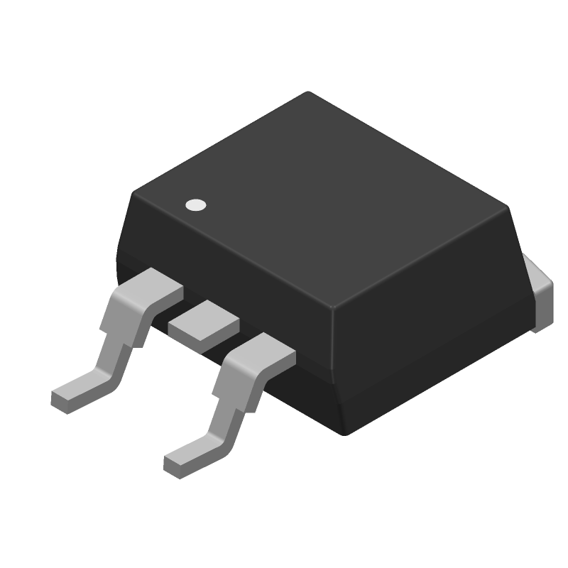
3D Model
Available Download Formats
By downloading CAD models, you agree to our Terms & Conditions and Privacy Policy
N-Channel Power Trench® MOSFET 75V, 14A, 47mΩ, D2PAK-3 / TO-263-2, 800-REEL
Tip: Data for a part may vary between manufacturers. You can filter for manufacturers on the top of the page next to the part image and part number.
FDB3502 by onsemi is a Power Field-Effect Transistor.
Power Field-Effect Transistors are under the broader part category of Transistors.
A transistor is a small semiconductor device used to amplify, control, or create electrical signals. When selecting a transistor, factors such as voltage, current rating, gain, and power dissipation must be considered, with common types. Read more about Transistors on our Transistors part category page.
| Part # | Distributor | Description | Stock | Price | Buy | |
|---|---|---|---|---|---|---|
|
DISTI #
08N9272
|
Newark | Fet 75V 47.0 Mohm D2Pak/Reel Rohs Compliant: Yes |Onsemi FDB3502 RoHS: Compliant Min Qty: 800 Package Multiple: 1 Date Code: 0 Container: Tape & Reel | 0 |
|
$1.0200 / $1.2700 | Buy Now |
|
DISTI #
FDB3502CT-ND
|
DigiKey | MOSFET N-CH 75V 6A/14A TO263AB Min Qty: 1 Lead time: 15 Weeks Container: Digi-Reel®, Cut Tape (CT), Tape & Reel (TR) |
471 In Stock |
|
$1.0529 / $2.4000 | Buy Now |
|
DISTI #
FDB3502
|
Avnet Americas | N-Channel Power Trench? MOSFET 75V, 14A, 47mO - Tape and Reel (Alt: FDB3502) COO: China RoHS: Compliant Min Qty: 1600 Package Multiple: 800 Container: Tape & Reel | 0 |
|
RFQ | |
|
|
Rochester Electronics | Power Field-Effect Transistor, 6A, 75V, 0.047ohm, N-Channel, MOSFET, TO-263AB RoHS: Not Compliant Status: Active Min Qty: 1 | 6764 |
|
$0.5894 / $0.9506 | Buy Now |
|
DISTI #
FDB3502
|
Richardson RFPD | POWER MOSFET TRANSISTOR RoHS: Compliant Min Qty: 1600 | 0 |
|
$0.7000 | Buy Now |
|
|
Flip Electronics | Stock, Ship Today | 480 |
|
RFQ | |
|
|
LCSC | 75V 14A 47m10V6A 41W One N-channel TO-263AB Single FETs MOSFETs RoHS | 15 |
|
$1.1203 / $1.8241 | Buy Now |
By downloading CAD models, you agree to our Terms & Conditions and Privacy Policy
|
|
FDB3502
onsemi
Buy Now
Datasheet
|
Compare Parts:
FDB3502
onsemi
N-Channel Power Trench® MOSFET 75V, 14A, 47mΩ, D2PAK-3 / TO-263-2, 800-REEL
|
| Pbfree Code | Yes | |
| Rohs Code | Yes | |
| Part Life Cycle Code | Obsolete | |
| Part Package Code | D2PAK-3 / TO-263-2 | |
| Package Description | Rohs Compliant Package-3 | |
| Manufacturer Package Code | 418AJ | |
| Reach Compliance Code | Not Compliant | |
| ECCN Code | EAR99 | |
| Avalanche Energy Rating (Eas) | 54 Mj | |
| Case Connection | Drain | |
| Configuration | Single With Built-In Diode | |
| DS Breakdown Voltage-Min | 75 V | |
| Drain Current-Max (ID) | 6 A | |
| Drain-source On Resistance-Max | 0.047 Ω | |
| FET Technology | Metal-Oxide Semiconductor | |
| JEDEC-95 Code | TO-263AB | |
| JESD-30 Code | R-PSSO-G2 | |
| JESD-609 Code | e3 | |
| Moisture Sensitivity Level | 1 | |
| Number of Elements | 1 | |
| Number of Terminals | 2 | |
| Operating Mode | Enhancement Mode | |
| Operating Temperature-Max | 150 °C | |
| Package Body Material | Plastic/Epoxy | |
| Package Shape | Rectangular | |
| Package Style | Small Outline | |
| Peak Reflow Temperature (Cel) | 245 | |
| Polarity/Channel Type | N-Channel | |
| Power Dissipation-Max (Abs) | 41 W | |
| Pulsed Drain Current-Max (IDM) | 40 A | |
| Qualification Status | Not Qualified | |
| Surface Mount | Yes | |
| Terminal Finish | Matte Tin (Sn) - Annealed | |
| Terminal Form | Gull Wing | |
| Terminal Position | Single | |
| Time@Peak Reflow Temperature-Max (s) | 30 | |
| Transistor Application | Switching | |
| Transistor Element Material | Silicon |
The FDB3502 can operate from -40°C to 150°C, but the recommended operating temperature range is -20°C to 125°C for optimal performance.
The FDB3502 requires a bias voltage of 5V to 15V, and the recommended bias current is 10mA to 20mA. Ensure the bias voltage is stable and noise-free for optimal performance.
Use a 4-layer PCB with a solid ground plane and a thermal pad connected to a heat sink or a thermal via to ensure efficient heat dissipation. Keep the PCB layout compact and symmetrical to minimize noise and electromagnetic interference.
Use shielding, filtering, and grounding techniques to minimize EMI. Add decoupling capacitors and ferrite beads to the PCB to filter out high-frequency noise. Ensure the PCB layout is compact and symmetrical to reduce radiation.
The FDB3502's output requires a drive strength of 10mA to 20mA, and a termination resistance of 50Ω to 100Ω to ensure signal integrity and minimize reflections.