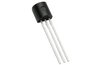
Part Details for KSC1730-R by Samsung Semiconductor
Results Overview of KSC1730-R by Samsung Semiconductor
- Distributor Offerings: (0 listings)
- Number of FFF Equivalents: (0 replacements)
- Tariff Estimator: (Available) NEW
- Number of Functional Equivalents: (0 options)
- CAD Models: (Request Part)
- Part Data Attributes: (Available)
- Reference Designs: (Not Available)
Tip: Data for a part may vary between manufacturers. You can filter for manufacturers on the top of the page next to the part image and part number.
KSC1730-R Information
KSC1730-R by Samsung Semiconductor is an RF Small Signal Bipolar Transistor.
RF Small Signal Bipolar Transistors are under the broader part category of Transistors.
A transistor is a small semiconductor device used to amplify, control, or create electrical signals. When selecting a transistor, factors such as voltage, current rating, gain, and power dissipation must be considered, with common types. Read more about Transistors on our Transistors part category page.
US Tariff Estimator: KSC1730-R by Samsung Semiconductor
Calculations from this tool are estimations only for imports into the United States. Please refer to the distributor or manufacturer and reference official US government sources and authorities to verify any final purchase costs.
KSC1730-R Part Data Attributes
|
|
KSC1730-R
Samsung Semiconductor
Buy Now
Datasheet
|
Compare Parts:
KSC1730-R
Samsung Semiconductor
RF Small Signal Bipolar Transistor, 0.05A I(C), 1-Element, Ultra High Frequency Band, Silicon, NPN, TO-92
|
| Part Life Cycle Code | Obsolete | |
| Part Package Code | TO-92 | |
| Package Description | To-92, 3 Pin | |
| Pin Count | 3 | |
| Reach Compliance Code | Unknown | |
| ECCN Code | EAR99 | |
| HTS Code | 8541.21.00.75 | |
| Collector Current-Max (IC) | 0.05 A | |
| Collector-Base Capacitance-Max | 1.5 Pf | |
| Collector-Emitter Voltage-Max | 15 V | |
| Configuration | Single | |
| DC Current Gain-Min (hFE) | 40 | |
| Highest Frequency Band | Ultra High Frequency Band | |
| JEDEC-95 Code | TO-92 | |
| JESD-30 Code | O-PBCY-T3 | |
| Number of Elements | 1 | |
| Number of Terminals | 3 | |
| Package Body Material | Plastic/Epoxy | |
| Package Shape | Round | |
| Package Style | Cylindrical | |
| Polarity/Channel Type | Npn | |
| Power Dissipation Ambient-Max | 0.25 W | |
| Qualification Status | Not Qualified | |
| Surface Mount | No | |
| Terminal Form | Through-Hole | |
| Terminal Position | Bottom | |
| Transistor Application | Amplifier | |
| Transistor Element Material | Silicon | |
| Transition Frequency-Nom (fT) | 1100 Mhz |