Part Details for STL9N60M2 by STMicroelectronics
Results Overview of STL9N60M2 by STMicroelectronics
- Distributor Offerings: (5 listings)
- Number of FFF Equivalents: (0 replacements)
- Tariff Estimator: (Not Available)
- Number of Functional Equivalents: (0 options)
- CAD Models: (Available)
- Part Data Attributes: (Available)
- Reference Designs: (Not Available)
Tip: Data for a part may vary between manufacturers. You can filter for manufacturers on the top of the page next to the part image and part number.
STL9N60M2 Information
STL9N60M2 by STMicroelectronics is a Power Field-Effect Transistor.
Power Field-Effect Transistors are under the broader part category of Transistors.
A transistor is a small semiconductor device used to amplify, control, or create electrical signals. When selecting a transistor, factors such as voltage, current rating, gain, and power dissipation must be considered, with common types. Read more about Transistors on our Transistors part category page.
Price & Stock for STL9N60M2
| Part # | Distributor | Description | Stock | Price | Buy | |
|---|---|---|---|---|---|---|
|
DISTI #
511-STL9N60M2
|
Mouser Electronics | MOSFETs N-channel 600 V, 0.76 Ohm typ., 4.8 A MDmesh M2 Power MOSFET in a PowerFLAT 5x6 RoHS: Compliant | 3882 |
|
$0.7140 / $2.4000 | Buy Now |
|
|
Future Electronics | N-Channel 600 V 4.8 A 860 mOhm SMT MDmesh M2 Power MOSFET 5 x 6 RoHS: Compliant pbFree: Yes Min Qty: 3000 Package Multiple: 3000 Lead time: 36 Weeks Container: Reel | 0Reel |
|
$1.6500 | Buy Now |
|
|
Future Electronics | N-Channel 600 V 4.8 A 860 mOhm SMT MDmesh M2 Power MOSFET 5 x 6 RoHS: Compliant pbFree: Yes Min Qty: 3000 Package Multiple: 3000 Lead time: 36 Weeks Container: Reel | 0Reel |
|
$1.6500 | Buy Now |
|
|
ComSIT USA | 600 V, 4.8 A, 0.76 OHM TYP MDMESH II PLUS LOW QG N-CHANNEL POWER MOSFET IN POWERFLAT 5 X 6 HV PACKAGE Power Field-Effect Transistor ECCN: EAR99 RoHS: Compliant |
|
|
RFQ | |
|
|
Chip Stock | N-channel 600 V, 0.76 Ohm typ., 4.8 A MDmesh M2 Power MOSFET in a PowerFLAT(TM) 5x6 HV package | 18570 |
|
RFQ |
STL9N60M2 CAD Models
-
3D Model
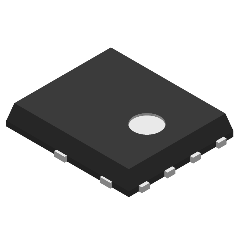
Available Download Formats
By downloading CAD models, you agree to our Terms & Conditions and Privacy Policy
STL9N60M2 Part Data Attributes
|
|
STL9N60M2
STMicroelectronics
Buy Now
Datasheet
|
Compare Parts:
STL9N60M2
STMicroelectronics
Power Field-Effect Transistor, 4.8A I(D), 600V, 0.86ohm, 1-Element, N-Channel, Silicon, Metal-oxide Semiconductor FET
|
| Rohs Code | Yes | |
| Part Life Cycle Code | Active | |
| ECCN Code | EAR99 | |
| Factory Lead Time | 14 Weeks | |
| Additional Feature | Bulk; 3000 | |
| Avalanche Energy Rating (Eas) | 30 Mj | |
| Case Connection | Drain | |
| Configuration | Single With Built-In Diode | |
| DS Breakdown Voltage-Min | 600 V | |
| Drain Current-Max (ID) | 4.8 A | |
| Drain-source On Resistance-Max | 0.86 Ω | |
| FET Technology | Metal-Oxide Semiconductor | |
| Feedback Cap-Max (Crss) | 0.68 Pf | |
| JESD-30 Code | S-PDSO-F8 | |
| Number of Elements | 1 | |
| Number of Terminals | 8 | |
| Operating Mode | Enhancement Mode | |
| Operating Temperature-Max | 150 °C | |
| Package Body Material | Plastic/Epoxy | |
| Package Shape | Rectangular | |
| Package Style | Small Outline | |
| Packing Method | Tr, 13 Inch | |
| Polarity/Channel Type | N-Channel | |
| Power Dissipation-Max (Abs) | 48 W | |
| Pulsed Drain Current-Max (IDM) | 3 A | |
| Surface Mount | Yes | |
| Terminal Form | Flat | |
| Terminal Position | Dual | |
| Transistor Application | Switching | |
| Transistor Element Material | Silicon |
STL9N60M2 Frequently Asked Questions (FAQ)
-
The maximum safe operating area (SOA) for the STL9N60M2 is not explicitly stated in the datasheet, but it can be estimated based on the device's thermal resistance and maximum junction temperature. A safe operating area can be determined by ensuring that the device's power dissipation does not exceed the maximum allowed value, taking into account the thermal resistance and maximum junction temperature.
-
To minimize switching losses, ensure that the gate drive voltage is sufficient (typically 10-15V) and the gate resistance is minimized (typically <10 ohms). Also, ensure that the gate drive circuit is capable of providing sufficient current to charge and discharge the gate capacitance quickly. A good gate drive design should also include a proper layout to minimize parasitic inductance and capacitance.
-
To minimize EMI, it is recommended to use a multi-layer PCB with a solid ground plane, and to keep the high-frequency switching nodes (e.g. drain and source) as close to the ground plane as possible. Additionally, use a shielded cable or a coaxial cable for the gate drive signal, and keep the PCB traces as short and direct as possible. A good layout should also include a common-mode choke or a ferrite bead to filter out high-frequency noise.
-
To protect the STL9N60M2 from overvoltage and overcurrent, use a voltage clamp or a transient voltage suppressor (TVS) to limit the voltage across the device. Additionally, use a current sense resistor and a comparator or an overcurrent protection IC to detect and respond to overcurrent conditions. A good design should also include a fuse or a polyfuse to protect against excessive current.
-
To ensure proper thermal management, use a heat sink with a thermal resistance of <1°C/W, and apply a thermal interface material (TIM) with a thermal conductivity of >5 W/m-K. Ensure good thermal contact between the device and the heat sink, and consider using a fan or a heat pipe to enhance heat dissipation. A good thermal design should also take into account the device's maximum junction temperature and the ambient temperature.