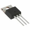
Part Details for STP3N60FI by STMicroelectronics
Results Overview of STP3N60FI by STMicroelectronics
- Distributor Offerings: (1 listing)
- Number of FFF Equivalents: (0 replacements)
- Tariff Estimator: (Available) NEW
- Number of Functional Equivalents: (0 options)
- CAD Models: (Request Part)
- Part Data Attributes: (Available)
- Reference Designs: (Not Available)
Tip: Data for a part may vary between manufacturers. You can filter for manufacturers on the top of the page next to the part image and part number.
STP3N60FI Information
STP3N60FI by STMicroelectronics is a Power Field-Effect Transistor.
Power Field-Effect Transistors are under the broader part category of Transistors.
A transistor is a small semiconductor device used to amplify, control, or create electrical signals. When selecting a transistor, factors such as voltage, current rating, gain, and power dissipation must be considered, with common types. Read more about Transistors on our Transistors part category page.
Price & Stock for STP3N60FI
| Part # | Distributor | Description | Stock | Price | Buy | |
|---|---|---|---|---|---|---|
|
|
Quest Components | TRANSISTOR,MOSFET,N-CHANNEL,600V V(BR)DSS,2.7A I(D),TO-220VAR | 1294 |
|
$0.5500 / $1.5000 | Buy Now |
US Tariff Estimator: STP3N60FI by STMicroelectronics
Calculations from this tool are estimations only for imports into the United States. Please refer to the distributor or manufacturer and reference official US government sources and authorities to verify any final purchase costs.
STP3N60FI Part Data Attributes
|
|
STP3N60FI
STMicroelectronics
Buy Now
Datasheet
|
Compare Parts:
STP3N60FI
STMicroelectronics
Power Field-Effect Transistor, 2.7A I(D), 600V, 2.2ohm, 1-Element, N-Channel, Silicon, Metal-oxide Semiconductor FET, TO-220AB
|
| Rohs Code | Yes | |
| Part Life Cycle Code | Obsolete | |
| Part Package Code | SFM | |
| Package Description | To-220, 3 Pin | |
| Pin Count | 3 | |
| ECCN Code | EAR99 | |
| HTS Code | 8541.29.00.95 | |
| Avalanche Energy Rating (Eas) | 370 Mj | |
| Case Connection | Isolated | |
| Configuration | Single With Built-In Diode | |
| DS Breakdown Voltage-Min | 600 V | |
| Drain Current-Max (ID) | 2.7 A | |
| Drain-source On Resistance-Max | 2.2 Ω | |
| FET Technology | Metal-Oxide Semiconductor | |
| Feedback Cap-Max (Crss) | 50 Pf | |
| JEDEC-95 Code | TO-220AB | |
| JESD-30 Code | R-PSFM-T3 | |
| JESD-609 Code | e3 | |
| Number of Elements | 1 | |
| Number of Terminals | 3 | |
| Operating Mode | Enhancement Mode | |
| Operating Temperature-Max | 150 °C | |
| Package Body Material | Plastic/Epoxy | |
| Package Shape | Rectangular | |
| Package Style | Flange Mount | |
| Polarity/Channel Type | N-Channel | |
| Power Dissipation Ambient-Max | 35 W | |
| Power Dissipation-Max (Abs) | 35 W | |
| Pulsed Drain Current-Max (IDM) | 14 A | |
| Qualification Status | Not Qualified | |
| Surface Mount | No | |
| Terminal Finish | Matte Tin (Sn) | |
| Terminal Form | Through-Hole | |
| Terminal Position | Single | |
| Transistor Application | Switching | |
| Transistor Element Material | Silicon | |
| Turn-off Time-Max (toff) | 45 Ns | |
| Turn-on Time-Max (ton) | 102 Ns |
STP3N60FI Frequently Asked Questions (FAQ)
-
The maximum safe operating area (SOA) for the STP3N60FI is not explicitly stated in the datasheet, but it can be estimated based on the device's thermal and electrical characteristics. A safe operating area can be determined by considering the device's maximum junction temperature, voltage, and current ratings, as well as its thermal impedance and switching characteristics.
-
To minimize switching losses, ensure that the gate drive voltage is sufficient (typically 10-15V) and the gate resistance is low (typically <10 ohms). Also, use a gate driver with a high current capability to quickly charge and discharge the gate capacitance. Additionally, consider using a gate driver with an integrated bootstrap diode to reduce power consumption.
-
To minimize parasitic inductance and capacitance, use a compact PCB layout with short, wide traces for the drain, source, and gate connections. Place the device close to the gate driver and use a ground plane to reduce inductance. Avoid using vias or narrow traces, and keep the drain and source connections separate to minimize capacitance.
-
To handle thermal management, ensure good heat sinking by using a heat sink with a low thermal resistance and a thermal interface material (TIM) with a low thermal impedance. Also, consider using a thermal pad or a heat spreader to dissipate heat away from the device. Monitor the device's junction temperature and adjust the heat sinking accordingly to prevent overheating.
-
To protect the device from electrostatic discharge (ESD), use ESD-sensitive handling procedures during assembly and storage. Implement ESD protection circuits, such as TVS diodes or ESD protection arrays, on the PCB to absorb ESD events. Also, consider using a device with built-in ESD protection, such as the STP3N60FI, which has a human-body model (HBM) ESD rating of 2kV.