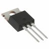
Part Details for STP50N06L by STMicroelectronics
Results Overview of STP50N06L by STMicroelectronics
- Distributor Offerings: (1 listing)
- Number of FFF Equivalents: (0 replacements)
- Tariff Estimator: (Available) NEW
- Number of Functional Equivalents: (0 options)
- CAD Models: (Request Part)
- Part Data Attributes: (Available)
- Reference Designs: (Not Available)
Tip: Data for a part may vary between manufacturers. You can filter for manufacturers on the top of the page next to the part image and part number.
STP50N06L Information
STP50N06L by STMicroelectronics is a Power Field-Effect Transistor.
Power Field-Effect Transistors are under the broader part category of Transistors.
A transistor is a small semiconductor device used to amplify, control, or create electrical signals. When selecting a transistor, factors such as voltage, current rating, gain, and power dissipation must be considered, with common types. Read more about Transistors on our Transistors part category page.
Price & Stock for STP50N06L
| Part # | Distributor | Description | Stock | Price | Buy | |
|---|---|---|---|---|---|---|
|
|
Quest Components | TRANSISTOR,MOSFET,N-CHANNEL,60V V(BR)DSS,50A I(D),TO-220 | 13317 |
|
$0.4200 / $1.2000 | Buy Now |
US Tariff Estimator: STP50N06L by STMicroelectronics
Calculations from this tool are estimations only for imports into the United States. Please refer to the distributor or manufacturer and reference official US government sources and authorities to verify any final purchase costs.
STP50N06L Part Data Attributes
|
|
STP50N06L
STMicroelectronics
Buy Now
Datasheet
|
Compare Parts:
STP50N06L
STMicroelectronics
Power Field-Effect Transistor, 50A I(D), 60V, 0.028ohm, 1-Element, N-Channel, Silicon, Metal-oxide Semiconductor FET, TO-220AB
|
| Pbfree Code | No | |
| Part Life Cycle Code | Active Unconfirmed | |
| Part Package Code | TO-220AB | |
| Package Description | To-220, 3 Pin | |
| Pin Count | 3 | |
| ECCN Code | EAR99 | |
| HTS Code | 8541.29.00.95 | |
| Avalanche Energy Rating (Eas) | 400 Mj | |
| Configuration | Single With Built-In Diode | |
| DS Breakdown Voltage-Min | 60 V | |
| Drain Current-Max (ID) | 50 A | |
| Drain-source On Resistance-Max | 0.028 Ω | |
| FET Technology | Metal-Oxide Semiconductor | |
| Feedback Cap-Max (Crss) | 300 Pf | |
| JEDEC-95 Code | TO-220AB | |
| JESD-30 Code | R-PSFM-T3 | |
| JESD-609 Code | e0 | |
| Number of Elements | 1 | |
| Number of Terminals | 3 | |
| Operating Mode | Enhancement Mode | |
| Operating Temperature-Max | 175 °C | |
| Package Body Material | Plastic/Epoxy | |
| Package Shape | Rectangular | |
| Package Style | Flange Mount | |
| Polarity/Channel Type | N-Channel | |
| Power Dissipation Ambient-Max | 150 W | |
| Power Dissipation-Max (Abs) | 150 W | |
| Pulsed Drain Current-Max (IDM) | 200 A | |
| Qualification Status | Not Qualified | |
| Surface Mount | No | |
| Terminal Finish | Tin Lead | |
| Terminal Form | Through-Hole | |
| Terminal Position | Single | |
| Transistor Application | Switching | |
| Transistor Element Material | Silicon | |
| Turn-on Time-Max (ton) | 195 Ns |
STP50N06L Frequently Asked Questions (FAQ)
-
The maximum safe operating area (SOA) for the STP50N06L is not explicitly stated in the datasheet, but it can be estimated based on the device's thermal and electrical characteristics. As a general rule, it's recommended to operate the device within the specified maximum ratings and avoid operating conditions that may cause excessive heat, voltage, or current stress.
-
To ensure proper thermal management, it's essential to provide a good thermal path from the device to a heat sink or the PCB. This can be achieved by using a thermal interface material (TIM) between the device and the heat sink, and ensuring that the heat sink is properly attached to the PCB. Additionally, the PCB should be designed to dissipate heat efficiently, and the device should be operated within its specified thermal ratings.
-
The recommended gate drive voltage for the STP50N06L is typically between 10V to 15V, depending on the specific application and switching frequency. However, it's essential to ensure that the gate drive voltage is within the specified maximum rating of 20V to avoid damaging the device.
-
To protect the STP50N06L from electrostatic discharge (ESD), it's essential to handle the device with care and follow proper ESD precautions during assembly and testing. This includes using ESD-safe materials, grounding personnel and equipment, and avoiding direct contact with the device's pins.
-
The maximum allowed voltage slew rate for the STP50N06L is not explicitly stated in the datasheet, but it's generally recommended to limit the voltage slew rate to 10V/ns or less to avoid excessive voltage stress and ensure reliable operation.