Part Details for STS3DPF20V by STMicroelectronics
Results Overview of STS3DPF20V by STMicroelectronics
- Distributor Offerings: (1 listing)
- Number of FFF Equivalents: (0 replacements)
- Tariff Estimator: (Not Available)
- Number of Functional Equivalents: (0 options)
- CAD Models: (Available)
- Part Data Attributes: (Available)
- Reference Designs: (Not Available)
Tip: Data for a part may vary between manufacturers. You can filter for manufacturers on the top of the page next to the part image and part number.
STS3DPF20V Information
STS3DPF20V by STMicroelectronics is a Power Field-Effect Transistor.
Power Field-Effect Transistors are under the broader part category of Transistors.
A transistor is a small semiconductor device used to amplify, control, or create electrical signals. When selecting a transistor, factors such as voltage, current rating, gain, and power dissipation must be considered, with common types. Read more about Transistors on our Transistors part category page.
Price & Stock for STS3DPF20V
| Part # | Distributor | Description | Stock | Price | Buy | |
|---|---|---|---|---|---|---|
|
|
Quest Components | POWER FIELD-EFFECT TRANSISTOR, 3A I(D), 20V, 0.135OHM, 2-ELEMENT, P-CHANNEL, SILICON, METAL-OXIDE SEMICONDUCTOR FET | 30 |
|
$0.9000 / $1.5000 | Buy Now |
STS3DPF20V CAD Models
-
Part Symbol
-
Footprint
-
3D Model
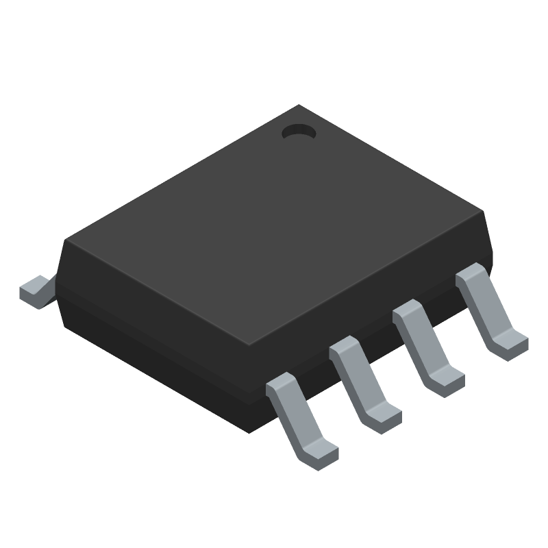
Available Download Formats
By downloading CAD models, you agree to our Terms & Conditions and Privacy Policy
STS3DPF20V Part Data Attributes
|
|
STS3DPF20V
STMicroelectronics
Buy Now
Datasheet
|
Compare Parts:
STS3DPF20V
STMicroelectronics
Power Field-Effect Transistor, 3A I(D), 20V, 0.135ohm, 2-Element, P-Channel, Silicon, Metal-oxide Semiconductor FET
|
| Rohs Code | Yes | |
| Part Life Cycle Code | Obsolete | |
| Part Package Code | SOT | |
| Package Description | Sop-8 | |
| Pin Count | 8 | |
| ECCN Code | EAR99 | |
| Additional Feature | Low Threshold | |
| Configuration | Separate, 2 Elements With Built-In Diode | |
| DS Breakdown Voltage-Min | 20 V | |
| Drain Current-Max (ID) | 3 A | |
| Drain-source On Resistance-Max | 0.135 Ω | |
| FET Technology | Metal-Oxide Semiconductor | |
| Feedback Cap-Max (Crss) | 30 Pf | |
| JESD-30 Code | R-PDSO-G8 | |
| JESD-609 Code | e4 | |
| Moisture Sensitivity Level | 1 | |
| Number of Elements | 2 | |
| Number of Terminals | 8 | |
| Operating Mode | Enhancement Mode | |
| Operating Temperature-Max | 150 °C | |
| Operating Temperature-Min | -55 °C | |
| Package Body Material | Plastic/Epoxy | |
| Package Shape | Rectangular | |
| Package Style | Small Outline | |
| Polarity/Channel Type | P-Channel | |
| Power Dissipation-Max (Abs) | 2 W | |
| Pulsed Drain Current-Max (IDM) | 12 A | |
| Qualification Status | Not Qualified | |
| Surface Mount | Yes | |
| Terminal Finish | Nickel/Palladium/Gold (Ni/Pd/Au) | |
| Terminal Form | Gull Wing | |
| Terminal Position | Dual | |
| Transistor Application | Switching | |
| Transistor Element Material | Silicon |
STS3DPF20V Frequently Asked Questions (FAQ)
-
STMicroelectronics recommends a PCB layout with a thermal pad connected to a large copper area on the bottom layer, and multiple vias to dissipate heat efficiently. A minimum of 2oz copper thickness is recommended.
-
To ensure reliable operation at high temperatures, it's essential to follow the recommended thermal design guidelines, use a suitable thermal interface material, and ensure good airflow around the device. Additionally, consider using a heat sink or a thermal shield to reduce the junction temperature.
-
The maximum allowed voltage on the enable pin (EN) is 6V, which is higher than the recommended operating voltage of 3.3V or 5V. However, it's essential to ensure that the voltage on the EN pin does not exceed the voltage on the VCC pin.
-
Yes, the STS3DPF20V is suitable for high-frequency switching applications up to 100 kHz. However, it's essential to consider the device's switching characteristics, such as rise and fall times, and ensure that the application's switching frequency does not exceed the device's maximum rating.
-
To protect the device from overvoltage and overcurrent conditions, consider using external protection components such as TVS diodes, zener diodes, or fuses. Additionally, ensure that the device is operated within its recommended operating conditions and that the PCB design includes adequate clearance and creepage distances.