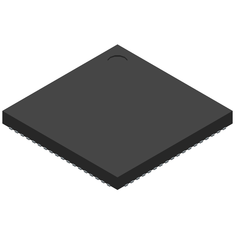
Part Details for AD9121BCPZRL by Analog Devices Inc
Results Overview of AD9121BCPZRL by Analog Devices Inc
- Distributor Offerings: (6 listings)
- Number of FFF Equivalents: (0 replacements)
- Tariff Estimator: (Available) NEW
- Number of Functional Equivalents: (0 options)
- CAD Models: (Available)
- Part Data Attributes: (Available)
- Reference Designs: (Not Available)
Tip: Data for a part may vary between manufacturers. You can filter for manufacturers on the top of the page next to the part image and part number.
AD9121BCPZRL Information
AD9121BCPZRL by Analog Devices Inc is a Digital to Analog Converter.
Digital to Analog Converters are under the broader part category of Converters.
A converter is an electrical circuit that transforms electric energy into a different form that will support a elecrical load needed by a device. Read more about Converters on our Converters part category page.
Price & Stock for AD9121BCPZRL
| Part # | Distributor | Description | Stock | Price | Buy | |
|---|---|---|---|---|---|---|
|
DISTI #
AD9121BCPZRLTR-ND
|
DigiKey | IC DAC 14BIT A-OUT 72LFCSP Min Qty: 2000 Lead time: 10 Weeks Container: Tape & Reel (TR) | Temporarily Out of Stock |
|
$51.0250 | Buy Now |
|
DISTI #
584-AD9121BCPZR
|
Mouser Electronics | Digital to Analog Converters - DAC 14 Bit Dual Signal Proc DAC RoHS: Compliant | 0 |
|
$51.0300 | Order Now |
|
|
Analog Devices Inc | 14 Bit Dual Signal Proc DAC Min Qty: 2000 Package Multiple: 2000 | 0 |
|
$37.8800 / $72.7000 | Buy Now |
|
|
Rochester Electronics | D/A Converter, 1 Func, Serial Input Loading, 0.02us Settling Time RoHS: Compliant Status: Active Min Qty: 1 | 3113 |
|
$42.9700 / $53.7100 | Buy Now |
|
|
Chip Stock | Dual,14-Bit,1230MSPS,TxDAC+Digital-to-AnalogConverter | 8040 |
|
RFQ | |
|
|
Win Source Electronics | IC DAC 14BIT A-OUT 72LFCSP | 6540 |
|
$33.5664 / $43.3566 | Buy Now |
US Tariff Estimator: AD9121BCPZRL by Analog Devices Inc
Calculations from this tool are estimations only for imports into the United States. Please refer to the distributor or manufacturer and reference official US government sources and authorities to verify any final purchase costs.
Part Details for AD9121BCPZRL
AD9121BCPZRL CAD Models
-
Part Symbol
-
Footprint
-
3D Model
Available Download Formats
By downloading CAD models, you agree to our Terms & Conditions and Privacy Policy
AD9121BCPZRL Part Data Attributes
|
|
AD9121BCPZRL
Analog Devices Inc
Buy Now
Datasheet
|
Compare Parts:
AD9121BCPZRL
Analog Devices Inc
D/A Converter, 1 Func, Serial Input Loading, 0.02us Settling Time
|
| Pbfree Code | No | |
| Rohs Code | Yes | |
| Part Life Cycle Code | Active | |
| Package Description | Hvqccn, Lcc72,.39sq,20 | |
| Pin Count | 72 | |
| Manufacturer Package Code | CP-72-7 | |
| Reach Compliance Code | Compliant | |
| ECCN Code | EAR99 | |
| HTS Code | 8542.39.00.01 | |
| Analog Output Voltage-Max | 1 V | |
| Analog Output Voltage-Min | -1 V | |
| Converter Type | D/A Converter | |
| Input Bit Code | 2'S COMPLEMENT | |
| Input Format | Serial | |
| JESD-30 Code | S-XQCC-N72 | |
| JESD-609 Code | e3 | |
| Length | 10 Mm | |
| Moisture Sensitivity Level | 3 | |
| Number of Bits | 14 | |
| Number of Functions | 1 | |
| Number of Terminals | 72 | |
| Operating Temperature-Max | 85 °C | |
| Operating Temperature-Min | -40 °C | |
| Package Body Material | Unspecified | |
| Package Code | HVQCCN | |
| Package Equivalence Code | LCC72,.39SQ,20 | |
| Package Shape | Square | |
| Package Style | Chip Carrier, Heat Sink/Slug, Very Thin Profile | |
| Qualification Status | Not Qualified | |
| Seated Height-Max | 1 Mm | |
| Settling Time-Nom (tstl) | 0.02 µS | |
| Supply Current-Max | 495 Ma | |
| Supply Voltage-Nom | 3.3 V | |
| Surface Mount | Yes | |
| Technology | Cmos | |
| Temperature Grade | Industrial | |
| Terminal Finish | Matte Tin (Sn) | |
| Terminal Form | No Lead | |
| Terminal Pitch | 0.5 Mm | |
| Terminal Position | Quad | |
| Width | 10 Mm |
AD9121BCPZRL Frequently Asked Questions (FAQ)
-
The AD9121 requires careful PCB layout and design to ensure optimal performance. Analog Devices provides a recommended PCB layout and design guide in the AD9121 evaluation board documentation, which includes guidelines for signal routing, power supply decoupling, and thermal management.
-
The AD9121's clocking and synchronization can be optimized by carefully selecting the clock source, configuring the clock multiplier, and adjusting the synchronization settings. Analog Devices provides application notes and technical support to help with this process.
-
The AD9121's internal DAC calibration is convenient but may not provide the same level of accuracy as external calibration. External calibration provides more flexibility and accuracy but requires additional circuitry and complexity. The choice depends on the specific application requirements and trade-offs.
-
Proper synchronization of the AD9121's digital interface with an FPGA or ASIC requires careful attention to clock domain crossing, data alignment, and synchronization protocols. Analog Devices provides guidelines and recommendations for specific interfaces, such as JESD204B or LVDS.
-
The AD9121 requires proper thermal management to ensure reliable operation. This includes providing adequate heat sinking, airflow, and thermal interface materials. Analog Devices provides thermal management guidelines and recommendations for the AD9121.
