
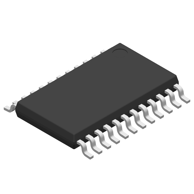
| Part Number | Manufacturer | Composite Price | Description | Compare |
|---|---|---|---|---|
| CDCE949PWR | Texas Instruments | $2.5286 | Video Clock Generator, 230MHz, CMOS, PDSO24 | CDCE949PW vs CDCE949PWR |
| CDCE949PWRG4 | Texas Instruments | Check for Price | Video Clock Generator, 230MHz, CMOS, PDSO24 | CDCE949PW vs CDCE949PWRG4 |
Part Details for CDCE949PW by Texas Instruments
Results Overview of CDCE949PW by Texas Instruments
- Distributor Offerings: (15 listings)
- Number of FFF Equivalents: (2 replacements)
- Tariff Estimator: (Available) NEW
- Number of Functional Equivalents: (2 options)
- CAD Models: (Available)
- Part Data Attributes: (Available)
- Reference Designs: (Not Available)
Tip: Data for a part may vary between manufacturers. You can filter for manufacturers on the top of the page next to the part image and part number.
Applications
Industrial Automation
Financial Technology (Fintech)
CDCE949PW Information
CDCE949PW by Texas Instruments is a Clock Generator.
Clock Generators are under the broader part category of Microcontrollers and Processors.
Microcontrollers (MCUs) are small, low-power integrated circuits used to control embedded systems. Microcontrollers are primarily used to automate and control devices. Read more about Microcontrollers and Processors on our Microcontrollers and Processors part category page.
Available Datasheets
| Part # | Manufacturer | Description | Datasheet |
|---|---|---|---|
| CDCE949PW | Texas Instruments | Programmable 4-PLL VCXO Clock Synthesizer with 2.5V or 3.3V LVCMOS Outputs 24-TSSOP -40 to 85 | |
| CDCE949PWR | Texas Instruments | Programmable 4-PLL VCXO Clock Synthesizer with 2.5V or 3.3V LVCMOS Outputs 24-TSSOP -40 to 85 | |
| CDCE949PWG4 | Texas Instruments | Programmable 4-PLL VCXO Clock Synthesizer with 2.5V or 3.3V LVCMOS Outputs 24-TSSOP -40 to 85 |
Price & Stock for CDCE949PW
| Part # | Distributor | Description | Stock | Price | Buy | |
|---|---|---|---|---|---|---|
|
DISTI #
296-21984-ND
|
DigiKey | IC PLL CLOCK GENERATOR 24TSSOP Min Qty: 1 Container: Tube |
0 Tube |
|
$4.6978 / $7.9500 | Buy Now |
|
DISTI #
V99:2348_07248264
|
Arrow Electronics | Clock Generator 8MHz to 160MHz-IN 230MHz-OUT 24-Pin TSSOP Tube COO: Malaysia RoHS: Compliant Min Qty: 1 Package Multiple: 1 Lead time: 26 Weeks Date Code: 2250 | Americas - 159 |
|
$3.8523 / $7.2754 | Buy Now |
|
DISTI #
595-CDCE949PW
|
Mouser Electronics | Clock Synthesizer / Jitter Cleaner Progr 4-PLL VCXO Clo ck Synth A 595-CDCE A 595-CDCE949PWR RoHS: Compliant | 202 |
|
$4.5500 / $8.1100 | Buy Now |
|
DISTI #
85976514
|
Verical | Clock Generator 8MHz to 160MHz-IN 230MHz-OUT 24-Pin TSSOP Tube RoHS: Compliant Min Qty: 70 Package Multiple: 1 Date Code: 1001 | Americas - 381 |
|
$4.3125 / $5.3875 | Buy Now |
|
DISTI #
87133239
|
Verical | Clock Generator 8MHz to 160MHz-IN 230MHz-OUT 24-Pin TSSOP Tube RoHS: Compliant Min Qty: 3 Package Multiple: 1 Date Code: 2250 | Americas - 159 |
|
$7.2754 | Buy Now |
|
|
Bristol Electronics | Clock Generator 8MHz to 160MHz-IN 230MHz-OUT 24-Pin TSSOP Tube | 61 |
|
RFQ | |
|
|
Quest Components | 114 |
|
$2.4360 / $5.2200 | Buy Now | |
|
|
Quest Components | 48 |
|
$1.8750 / $3.7500 | Buy Now | |
|
|
Rochester Electronics | Video Clock Generator, 230MHz, CMOS, PDSO24 RoHS: Compliant Status: Active Min Qty: 1 | 401 |
|
$3.4500 / $4.3100 | Buy Now |
|
DISTI #
V99:2348_07248264
|
Arrow Electronics | Clock Generator 8MHz to 160MHz-IN 230MHz-OUT 24-Pin TSSOP Tube COO: Malaysia RoHS: Compliant Min Qty: 1 Package Multiple: 1 Lead time: 26 Weeks Date Code: 2250 | Americas - 159 |
|
$3.8523 / $7.2754 | Buy Now |
US Tariff Estimator: CDCE949PW by Texas Instruments
Calculations from this tool are estimations only for imports into the United States. Please refer to the distributor or manufacturer and reference official US government sources and authorities to verify any final purchase costs.
CDCE949PW CAD Models
-
Part Symbol
-
Footprint
-
3D Model
Available Download Formats
By downloading CAD models, you agree to our Terms & Conditions and Privacy Policy
CDCE949PW Part Data Attributes
|
|
CDCE949PW
Texas Instruments
Buy Now
Datasheet
|
Compare Parts:
CDCE949PW
Texas Instruments
Video Clock Generator, 230MHz, CMOS, PDSO24
|
| Pbfree Code | Yes | |
| Rohs Code | Yes | |
| Part Life Cycle Code | Active | |
| Part Package Code | TSSOP | |
| Pin Count | 24 | |
| ECCN Code | EAR99 | |
| HTS Code | 8542.39.00.90 | |
| JESD-30 Code | R-PDSO-G24 | |
| JESD-609 Code | e4 | |
| Length | 7.8 Mm | |
| Moisture Sensitivity Level | 1 | |
| Number of Terminals | 24 | |
| Operating Temperature-Max | 85 °C | |
| Operating Temperature-Min | -40 °C | |
| Output Clock Frequency-Max | 230 Mhz | |
| Package Body Material | Plastic/Epoxy | |
| Package Code | TSSOP | |
| Package Equivalence Code | TSSOP20,.25 | |
| Package Shape | Rectangular | |
| Package Style | Small Outline, Thin Profile, Shrink Pitch | |
| Peak Reflow Temperature (Cel) | 260 | |
| Primary Clock/Crystal Frequency-Nom | 32 Mhz | |
| Qualification Status | Not Qualified | |
| Seated Height-Max | 1.2 Mm | |
| Supply Current-Max | 38 Ma | |
| Supply Voltage-Max | 3.6 V | |
| Supply Voltage-Min | 2.3 V | |
| Supply Voltage-Nom | 1.8 V | |
| Surface Mount | Yes | |
| Technology | Cmos | |
| Temperature Grade | Industrial | |
| Terminal Finish | Nickel/Palladium/Gold (Ni/Pd/Au) | |
| Terminal Form | Gull Wing | |
| Terminal Pitch | 0.65 Mm | |
| Terminal Position | Dual | |
| Time@Peak Reflow Temperature-Max (s) | 30 | |
| Width | 4.4 Mm | |
| uPs/uCs/Peripheral ICs Type | Clock Generator, Video |
Alternate Parts for CDCE949PW
This table gives cross-reference parts and alternative options found for CDCE949PW. The Form Fit Function (FFF) tab will give you the options that are more likely to serve as direct pin-to-pin alternates or drop-in parts. The Functional Equivalents tab will give you options that are likely to match the same function of CDCE949PW, but it may not fit your design. Always verify details of parts you are evaluating, as these parts are offered as suggestions for what you are looking for and are not guaranteed.
CDCE949PW Frequently Asked Questions (FAQ)
-
The recommended power-up sequence is to apply VCC first, followed by VDD, and then the input clock signal. This ensures proper device operation and prevents potential latch-up conditions.
-
To ensure the CDCE949PW is in a known state after power-up, assert the reset pin (RST) low for at least 10 ns to reset the device. Then, release the reset pin to allow the device to start operating normally.
-
The CDCE949PW can support input clock frequencies up to 200 MHz. However, the maximum frequency may vary depending on the specific application and output frequency requirements.
-
To optimize the CDCE949PW for low power consumption, ensure that the input clock signal is clean and free of noise, use the lowest possible input clock frequency, and disable any unused outputs. Additionally, consider using the device's power-down mode when not in use.
-
To ensure proper operation and minimize noise, follow good PCB layout and routing practices, such as keeping clock signals away from analog signals, using short traces, and avoiding vias and right-angle turns.