| Part Number | Manufacturer | Composite Price | Description | Compare |
|---|---|---|---|---|
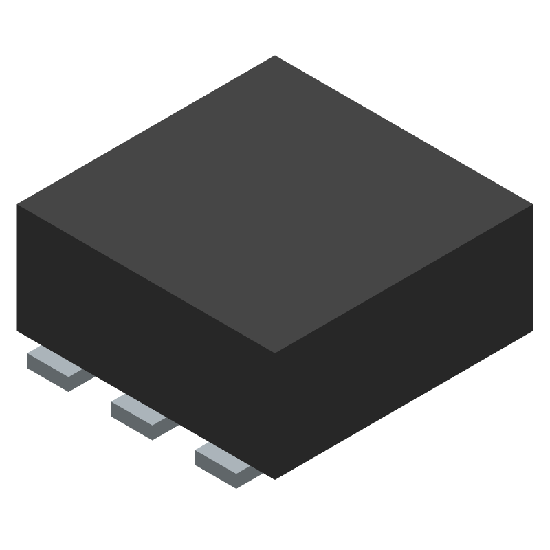
| CSD17313Q2T | Texas Instruments | $0.3002 | Power Field-Effect Transistor, 5A I(D), 30V, 0.042ohm, 1-Element, N-Channel, Silicon, Metal-oxide Semiconductor FET | CSD17313Q2 vs CSD17313Q2T |
Part Details for CSD17313Q2 by Texas Instruments
Results Overview of CSD17313Q2 by Texas Instruments
- Distributor Offerings: (26 listings)
- Number of FFF Equivalents: (1 replacement)
- Tariff Estimator: (Available) NEW
- Number of Functional Equivalents: (2 options)
- CAD Models: (Available)
- Part Data Attributes: (Available)
- Reference Designs: (Available)
Tip: Data for a part may vary between manufacturers. You can filter for manufacturers on the top of the page next to the part image and part number.
Applications
Energy and Power Systems
Transportation and Logistics
Renewable Energy
Automotive
CSD17313Q2 Information
CSD17313Q2 by Texas Instruments is a Power Field-Effect Transistor.
Power Field-Effect Transistors are under the broader part category of Transistors.
A transistor is a small semiconductor device used to amplify, control, or create electrical signals. When selecting a transistor, factors such as voltage, current rating, gain, and power dissipation must be considered, with common types. Read more about Transistors on our Transistors part category page.
Price & Stock for CSD17313Q2
| Part # | Distributor | Description | Stock | Price | Buy | |
|---|---|---|---|---|---|---|
|
DISTI #
29AH3828
|
Newark | Mosfet, N Ch, 30V, 5A, Son-6, |Texas Instruments CSD17313Q2 RoHS: Compliant Min Qty: 5 Package Multiple: 1 Date Code: 0 Container: Cut Tape | 1140 |
|
$0.2180 / $0.7960 | Buy Now |
|
DISTI #
29AH3828RL
|
Newark | Mosfet, N Ch, 30V, 5A, Son-6, |Texas Instruments CSD17313Q2 RoHS: Compliant Min Qty: 100 Package Multiple: 1 Date Code: 0 Container: Tape & Reel | 1140 |
|
$0.2180 / $0.3250 | Buy Now |
|
DISTI #
296-27233-1-ND
|
DigiKey | MOSFET N-CH 30V 5A 6WSON Min Qty: 1 Container: Cut Tape |
12281 Cut Tape |
|
$0.2436 / $0.8000 | Buy Now |
|
DISTI #
296-27233-6-ND
|
DigiKey | MOSFET N-CH 30V 5A 6WSON Min Qty: 1 Container: Digi-Reel |
12281 Digi-Reel® |
|
$0.2436 / $0.8000 | Buy Now |
|
DISTI #
296-27233-2-ND
|
DigiKey | MOSFET N-CH 30V 5A 6WSON Min Qty: 3000 Container: Tape & Reel |
12281 Tape & Reel |
|
$0.1640 / $0.1878 | Buy Now |
|
DISTI #
P02:6590_15779266
|
Arrow Electronics | Trans MOSFET N-CH Si 30V 7.3A 6-Pin WSON EP T/R RoHS: Compliant Min Qty: 10 Package Multiple: 1 Date Code: 2228 Container: Cut Strips | Asia - 1165 |
|
$0.1507 / $0.3390 | Buy Now |
|
DISTI #
V72:2272_07248766
|
Arrow Electronics | Trans MOSFET N-CH Si 30V 7.3A 6-Pin WSON EP T/R COO: Malaysia RoHS: Compliant Min Qty: 1 Package Multiple: 1 Lead time: 16 Weeks Date Code: 2228 Container: Cut Strips | Americas - 550 |
|
$0.1512 / $0.5991 | Buy Now |
|
DISTI #
595-CSD17313Q2
|
Mouser Electronics | MOSFETs 30V N Channel NexFET Power MOSFET A 595- A 595-CSD17313Q2T RoHS: Compliant | 16710 |
|
$0.1530 / $0.8000 | Buy Now |
|
DISTI #
93862089
|
Verical | Trans MOSFET N-CH Si 30V 7.3A 6-Pin WSON EP T/R RoHS: Compliant Min Qty: 10 Package Multiple: 1 Date Code: 2228 | Americas - 1165 |
|
$0.1507 / $0.3390 | Buy Now |
|
DISTI #
63258680
|
Verical | Trans MOSFET N-CH Si 30V 7.3A 6-Pin WSON EP T/R RoHS: Compliant Min Qty: 41 Package Multiple: 1 Date Code: 2228 | Americas - 550 |
|
$0.1512 / $0.3312 | Buy Now |
US Tariff Estimator: CSD17313Q2 by Texas Instruments
Calculations from this tool are estimations only for imports into the United States. Please refer to the distributor or manufacturer and reference official US government sources and authorities to verify any final purchase costs.
CSD17313Q2 CAD Models
-
Part Symbol
-
Footprint
-
3D Model
Available Download Formats
By downloading CAD models, you agree to our Terms & Conditions and Privacy Policy
CSD17313Q2 Part Data Attributes
|
|
CSD17313Q2
Texas Instruments
Buy Now
Datasheet
|
Compare Parts:
CSD17313Q2
Texas Instruments
Power Field-Effect Transistor, 5A I(D), 30V, 0.042ohm, 1-Element, N-Channel, Silicon, Metal-oxide Semiconductor FET
|
| Pbfree Code | Yes | |
| Rohs Code | Yes | |
| Part Life Cycle Code | Active | |
| Pin Count | 8 | |
| ECCN Code | EAR99 | |
| HTS Code | 8541.29.00.95 | |
| Avalanche Energy Rating (Eas) | 18 Mj | |
| Case Connection | Drain | |
| Configuration | Single With Built-In Diode | |
| DS Breakdown Voltage-Min | 30 V | |
| Drain Current-Max (ID) | 5 A | |
| Drain-source On Resistance-Max | 0.042 Ω | |
| FET Technology | Metal-Oxide Semiconductor | |
| Feedback Cap-Max (Crss) | 17 Pf | |
| JESD-30 Code | R-PDSO-N8 | |
| JESD-609 Code | e4 | |
| Moisture Sensitivity Level | 1 | |
| Number of Elements | 1 | |
| Number of Terminals | 6 | |
| Operating Mode | Enhancement Mode | |
| Operating Temperature-Max | 150 °C | |
| Operating Temperature-Min | -55 °C | |
| Package Body Material | Plastic/Epoxy | |
| Package Shape | Rectangular | |
| Package Style | Small Outline | |
| Peak Reflow Temperature (Cel) | 260 | |
| Polarity/Channel Type | N-Channel | |
| Power Dissipation-Max (Abs) | 17 W | |
| Pulsed Drain Current-Max (IDM) | 20 A | |
| Qualification Status | Not Qualified | |
| Surface Mount | Yes | |
| Terminal Finish | Nickel/Palladium/Gold (Ni/Pd/Au) | |
| Terminal Form | No Lead | |
| Terminal Position | Dual | |
| Time@Peak Reflow Temperature-Max (s) | 30 | |
| Transistor Application | Switching | |
| Transistor Element Material | Silicon |
Alternate Parts for CSD17313Q2
This table gives cross-reference parts and alternative options found for CSD17313Q2. The Form Fit Function (FFF) tab will give you the options that are more likely to serve as direct pin-to-pin alternates or drop-in parts. The Functional Equivalents tab will give you options that are likely to match the same function of CSD17313Q2, but it may not fit your design. Always verify details of parts you are evaluating, as these parts are offered as suggestions for what you are looking for and are not guaranteed.
Resources and Additional Insights for CSD17313Q2
Reference Designs related to CSD17313Q2
-
Automotive Discrete SBC Pre-Boost: Post-Buck With CAN Reference Design
The TIDA-01429 reference design implements a wideinput voltage boost controller: followed by a wide input voltage buck converter set to 5.0 V. The 5.0 V supply is used for powering a Controller Area Network (CAN) transceiver and a compact fixed 3.3 V linear drop-out (LDO) regulator for supplying the C2000 microcontroller. This design has been tested for CISPR 25 radiated emissions per absorber lined shielded enclosure (ALSE) method: CISPR25 conducted emissions via the voltage method: and for immunity to Bulk Current Injection (BCI) per ISO 11452-4: all with CAN communication operating at 500 KBPS. This is a electromagnetic compliance (EMC) vetted 3-stage power tree with controller area network (CAN) reference design that can be used in many automotive applications requiring operation with input voltages as low as 3.5 V.A system basis chip (SBC) is an integrated circuit (IC) that combines many typical building blocks of a system: which includes transceivers: linear regulators: and switching regulators. While these integrated devices can offer size and cost savings in a number of applications: the integrated devices do not work in every case. For applications where an SBC is not a good fit: it might be beneficial to build a discrete implementation of these aforementioned building blocks thus making a discrete SBC.
-
Flexible High Current IGBT Gate Driver with Reinforced Digital Isolator Reference Design
The TIDA-00448 reference design is an isolated IGBT gate driver with bipolar gate voltages intended for driving high power IGBT’s requiring high peak gate current up to 40 A. TI’s NexFET power blocks which scales in this range: with same package: enables single design to be used for multiple drive platforms with different power ratings. A Digital isolator is used to achieve reinforced isolation with transient surge rating of 8kV and 50kV CMTI. The design incorporates DESAT protection using a fast transient response comparator. The DESAT detection threshold and the soft turn-off time are configurable. The design can interface with PWMs from 3.3 V and 5 V MCUs along with fault: reset and UVLO feedbacks.
-
16-Bit 1-GSPS Digitizer Reference Design with AC and DC Coupled Fixed Gain Amplifier
This reference design discusses the use and performance of the Ultra-Wideband: Fixed-gain high-speed amplifier: the LMH3401 to drive the high-speed analog-to-digital converter (ADC): the ADS54J60 device. Different options for common-mode voltages: power supplies: and interfaces are discussed and measued: including AC-coupling and DC-coupling: to meet the requirements of a variety of applications.
-
USB Type-A Plug to USB Type-C Receptacle SuperSpeed MUX With DFP Controller Reference Design
The TIDA-00890 Dongle is designed to evaluate HD3SS3220 devices for DFP implementations. This reference design can also be used as a hardware reference design for any implementation using the HD3SS3220 with a USB-C™ connector. The layout files can be used as a guideline to implement the TUSB321A HD3SS3220 with illustrations of the routing/placement rules. The reference design includes on-board USB Type-A plug to connect to legacy USB systems. Please note that the design may include test components for evaluation purposes not applicable for production.
-
Audio Boom Box/Portable Speaker Reference Design with Efficient Boost Converter.
PMP9491 is a 30W highly efficient and compact Portable Speaker/Audio Boom Box reference Design which can be used in 15W +15W Stereo or 30W Woofer Applications. The Power Source for the Design is 1 or 2 Li ion in Series . The design is broadly divided into three main stages:Highly efficient Single-Phase Non Synchronous Boost Converter using the LM3481 controller IC. The design accepts an input voltage of 3.3Vin to 9Vin and provides an output of 12 V capable of supplying 2.5A of continuous current to the load. The peak efficency acheived is 95 percent .15W+15W Stereo Audio Amplifier with TPA3118D2 Class D device. Very Low Cost Stereo Inputs to Woofer Bass Input Conversion.Battery Charger bq24133 : 2.5A Synchronous Switch-Mode Li-Ion/Li-Polymer Stand-Alone Battery Charger with Integrated MOSFETs and Power Path Selector.
-
Automotive Pre-Buck: Post-Boost With CAN Discrete SBC Reference Design
The TIDA-01428 reference design implements a 1-A: wide-VIN: buck converter to 3.3 V followed by a compact: low-input voltage: fixed 5-V boost converter for powering a controller area network (CAN) physical layer interface. The design has been tested for CISPR 25 radiated emissions and conducted emissions using the voltage method and for immunity to bulk current injection (BCI) per ISO 11452-4 with CAN communication operating at 500 KBPS. The TIDA-01428 is an EMC-vetted power tree plus CAN reference design that can be used in many automotive applications. A system basis chip (SBC) is an integrated circuit (IC) that combines many typical building blocks of a system: which includes transceivers: linear regulators: and switching regulators. While these integrated devices can offer size and cost savings in a number of applications: the integrated devices do not work in every case. For applications where an SBC is not a good fit: it might be beneficial to build a discrete implementation of these aforementioned building blocks thus making a discrete SBC.
-
Optimizing LMH6554 to Drive High Speed ADCs
This reference design shows the ability of the high-speed amplifier: LMH6554: to perform single-ended to differential conversion to drive high-speed analog-to-digital converters (ADCs) while maintaining excellent noise and distortion performance. Performance versus input frequency is shown for both AC and DC coupled applications while interfaced to the ADS4449 quad: 250-MSPS: 14-bit ADC. Various options for common-mode voltages: power supplies: and interfaces are discussed and measured to meet the requirements of a variety of applications. Anti-aliasing filter examples are shown along with the performance improvements that they provide.
-
Wideband RF-to-Digital Complex Receiver-Feedback Signal Chain
This is a wideband complex-receiver reference design and evaluation platform that is ideally suited for use as a feedback receiver for transmitter digital predistortion. The EVM signal chain is ideal for high intermediate-frequency (IF) complex-feedback applications and contains a complex demodulator: TI’s LMH6521 dual-channel DVGA and ADS5402 12-bit 800-MSPS dual-channel ADC. By modifying the onboard filter components: the signal chain is configurable for a variety of frequency plans. The EVM also includes TI’s LMK04808 dual-PLL clock jitter cleaner and generator to provide an onboard low-noise clocking solution. The LMH6521 DVGA gain is controlled through the GUI or alternatively through the high speed connector with an FPGA.
-
Wideband Receiver Reference Design for Upstream DOCSIS 3.1 Applications
This reference design consists of an analog front-end (AFE) signal chain for wideband receiver applications using the LMH2832 digitally controlled variable gain amplifier (DVGA) and ADS54J40 analog-to-digital converter (ADC). The design is primarily targeted for upstream DOCSIS 3.1 receiver applications specified for cable modem termination systems (CMTS) and supports up to 196 MHz of upstream signal bandwidth. The circuit solves the filtering and analog signal processing requirements for the DOCSIS 3.1 standard: which makes it easier for system designers to readily incorporate the design on the CMTS-side of the upstream signal path.
-
Integrated 1-3S Standalone Battery Charger with EMI Compliance Reference Design
The PMP4397 is a battery charger module reference design suitable for 2-cell battery applications with a DC input of 4.5V – 15V. Detailed data for radiated emissions compliance is provided. The cell number could be trimmed by resistors over a range from 1-cell to 3-cells. A typical application is for 2-cells (8.4V/2000mAH).
-
TPS40400 Step-Down Regulator with PMBus Delivering 1.8V at 4A Reference Design
PMP11140 is a single-phase switching regulator accepting an input range of 4.5V to 13.2V and providing an output voltage of 1.8V capable of supplying 4A of current. This reference design shows 1.8Vout: 4A (3A without a fan) for CPU I/O and other applications in a 22cm by 12.6cm single sided footprint. A rich test interface including an on board dynamic load is provided.
-
16-Bit 1-GSPS Digitizer Reference Design with AC and DC Coupled Variable Gain Amplifier
This reference design discusses the use and performance of the Digital Variable-Gain high-speed amplifier: the LMH6401: to drive the high-speed analog-to-digital converter (ADC): the ADS54J60 device. Different options for common-mode voltages: power supplies: and interfaces are discussed and measued: including AC-coupling and DC-coupling: to meet the requirements of a variety of applications.
-
Automotive Dual Channel SiC MOSFET Gate Driver Reference Design with Two Level Turn-off Protection
This reference design is an automotive qualified isolated gate driver solution for driving Silicon Carbide (SiC) MOSFETs in half bridge configuration. The design includes two push pull bias supplies for the dual channel isolated gate driver respectively and each supply provides +15V and -4V output voltage and 1W output power. The gate driver is capable of delivering 4A source and 6A sink peak current. It implements reinforced isolation and can withstand 8kV Peak and 5.7kV RMS isolation voltage and >100V/ns common mode transient immunity (CMTI). The reference design contains the two-level turn-off circuit which protects the MOSFET from voltage overshoot during the short circuit scenario. The DESAT detection threshold and the delay time for second stage turn-off are configurable. The ISO7721-Q1 digital isolator is implemented for interfacing the signals of fault and reset. All designed on a two layer PCB board with a compact form factor of 40mm × 40mm.
-
3 - 4.2Vin: 1.35Vout @ 4A: DDR3 LV using the TPS51216
The PMP6807 reference design uses the TPS51216 to generate a low voltage DRR3 power supply. The VDDQ supply is 1.35V and capable of 4A. The VTT supply is generated using a source/sink LDO that is capable of 0.5A. The design also takes advantage of high performance compact MOSFETs (CSD17313Q2) to achieve efficiency over 90% for most of the load range.
-
12V Input Sync Buck 0.9V@7A
This reference design generates a 0.9V/7.5A output from a 12V input using the TPS40192 synchronous buck controller. The low Rds and fast switching of the CSD17313Q2 and CSD17308Q3 provide over 83% efficiency.
-
4-mA to 20-mA Loop Energy Harvester Reference Design
The TIDA-00649 reference design demonstrates energy harvesting from 4-mA to 20-mA loop-powered systems. The design is simple to insert into existing installations where it scavenges energy from the loop and generates a regulated output voltage. Furthermore: the circuit provides an analog output representing the actual loop current value. The insertion loss can be as low as 400 mV and can also be increased up to 2.85 V to address higher output power levels. All these features provide an easy way for powering wireless adapters (WirelessHART® : Bluetooth® low energy (BLE): and so forth): indicators: displays: Human Machine Interfaces (HMIs): and others for a seamless upgrade of existing 4-mA to 20-mA loop-powered systems.
-
Bi-directional: dual active bridge reference design for level 3 electric vehicle charging stations
This reference design provides an overview on the implementation of a single-phase dual active bridge (DAB) DC/DC converter. DAB topology offers advantages like soft-switching commutations: a decreased number of devices and high efficiency. The design is beneficial where power density: cost: weight: galvanic isolation: high voltage conversion ratio and reliability are critical factors: making it ideal for EV charging stations and energy storage applications. Modularity and symmetrical structure in DAB allow for stacking converters to achieve high power throughput and facilitate a bidirectional mode of operation to support battery charging and discharging applications.
-
Battery back-up switch: charger and monitor reference design
A complete battery back-up: charger and monitoring is implemented with this reference design. It includes switching between a 12/24-Vdc source and 12/24-V lead acid battery: constant current battery charging at 1A typical: battery maintenance float charge and monitoring circuits for the battery and input source.
-
Automotive 200-VA High Frequency Inverter Design
This design presents a low-cost: small size: robust 200-VA DC to AC inverter based on TI’s MSP430 and UCD8220-digitally managed push-pull controller. It is targetted towards car inverters and small-segment inverters for commercial applications. In this design: UCD8220 is used for a boost stage to get 250-V DC from a 12-V battery. The MSP430 acts as a host controller and provides a 100-kHz clock to UCD8220 and drives for output DC-AC bridge. This inverter has a peak efficiency of 90% and has natural cooling and does not require a fan for cooling.
-
DLP® auto headlight reference design
This reference design details the design of a control board for the DLP5531-Q1 DMD. The DLP5531-Q1 DMD is a spatial light modulator with over 1.3 million pixels that can steer light to create digitally controlled illumination distributions. The design shows a simplified power architecture with a reduced component count to save space and reduce cost. When combined with optics: an input video sources: and a computer or other means of control: this design can be use to demonstrate Adaptive Driving Beams: Glare-Free Beam Steering: Reflective Traffic Sign Dimming: Pedestrian Dimming: Symbol Projection: and OEM Branding.
1 - 5 of 20 reference designs
CSD17313Q2 Frequently Asked Questions (FAQ)
-
The maximum operating temperature range for the CSD17313Q2 is -40°C to 150°C.
-
To ensure proper biasing, connect the gate-source voltage (VGS) to a voltage source that is within the recommended operating range (typically 1.5V to 3.5V) and ensure the drain-source voltage (VDS) is within the recommended operating range (typically 1.5V to 12V).
-
To minimize parasitic inductance, use a compact PCB layout with short, wide traces for the drain, source, and gate connections. Avoid using vias or narrow traces, and keep the component placement close to the PCB surface.
-
To protect the CSD17313Q2 from ESD, use ESD-sensitive handling procedures, such as wearing an anti-static wrist strap or using an anti-static mat. Ensure the PCB is properly grounded, and use ESD-protection devices, such as TVS diodes, in the circuit design.
-
The recommended gate drive voltage for the CSD17313Q2 is typically 5V to 10V, depending on the specific application requirements. However, it's essential to consult the datasheet and application notes for specific guidance.