
| Part Number | Manufacturer | Composite Price | Description | Compare |
|---|---|---|---|---|
| CSD18511KTT | Texas Instruments | $0.8671 | Power Field-Effect Transistor, 110A I(D), 40V, 0.0042ohm, 1-Element, N-Channel, Silicon, Metal-oxide Semiconductor FET, TO-263AB | CSD18511KCS vs CSD18511KTT |
| CSD18511KTTT | Texas Instruments | $0.9788 | Power Field-Effect Transistor, 110A I(D), 40V, 0.0042ohm, 1-Element, N-Channel, Silicon, Metal-oxide Semiconductor FET, TO-263AB | CSD18511KCS vs CSD18511KTTT |
| STP190NF04 | STMicroelectronics | Check for Price | Power Field-Effect Transistor, 120A I(D), 40V, 0.0043ohm, 1-Element, N-Channel, Silicon, Metal-oxide Semiconductor FET, TO-220AB | CSD18511KCS vs STP190NF04 |
| STB190NF04-1 | STMicroelectronics | Check for Price | Power Field-Effect Transistor, 120A I(D), 40V, 0.0043ohm, 1-Element, N-Channel, Silicon, Metal-oxide Semiconductor FET, TO-262AA | CSD18511KCS vs STB190NF04-1 |
| STB200N4F3 | STMicroelectronics | Check for Price | Power Field-Effect Transistor, 120A I(D), 40V, 0.004ohm, 1-Element, N-Channel, Silicon, Metal-oxide Semiconductor FET | CSD18511KCS vs STB200N4F3 |
| IPB120N04S404ATMA1 | Infineon Technologies AG | Check for Price | Power Field-Effect Transistor, 120A I(D), 40V, 0.0036ohm, 1-Element, N-Channel, Silicon, Metal-oxide Semiconductor FET, TO-263AB | CSD18511KCS vs IPB120N04S404ATMA1 |
Part Details for CSD18511KCS by Texas Instruments
Results Overview of CSD18511KCS by Texas Instruments
- Distributor Offerings: (4 listings)
- Number of FFF Equivalents: (0 replacements)
- Tariff Estimator: (Available) NEW
- Number of Functional Equivalents: (6 options)
- CAD Models: (Available)
- Part Data Attributes: (Available)
- Reference Designs: (Not Available)
Tip: Data for a part may vary between manufacturers. You can filter for manufacturers on the top of the page next to the part image and part number.
Applications
Energy and Power Systems
Renewable Energy
CSD18511KCS Information
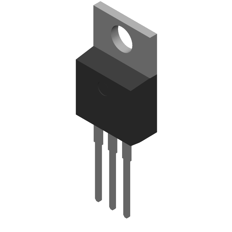
CSD18511KCS by Texas Instruments is a Power Field-Effect Transistor.
Power Field-Effect Transistors are under the broader part category of Transistors.
A transistor is a small semiconductor device used to amplify, control, or create electrical signals. When selecting a transistor, factors such as voltage, current rating, gain, and power dissipation must be considered, with common types. Read more about Transistors on our Transistors part category page.
Price & Stock for CSD18511KCS
| Part # | Distributor | Description | Stock | Price | Buy | |
|---|---|---|---|---|---|---|
|
DISTI #
CSD18511KCS-ND
|
DigiKey | MOSFET N-CH 40V 194A TO220-3 Min Qty: 1 Container: Tube |
301 Tube |
|
$0.8293 / $2.3900 | Buy Now |
|
DISTI #
595-CSD18511KCS
|
Mouser Electronics | MOSFETs 40-V N channel NexF ET power MOSFET si RoHS: Compliant | 281 |
|
$0.6830 / $2.3900 | Buy Now |
|
DISTI #
CSD18511KCS
|
TME | Transistor: N-MOSFET, unipolar, 40V, 110A, Idm: 400A, 188W, TO220-3 Min Qty: 1 | 0 |
|
$1.0100 / $2.1600 | RFQ |
|
|
Vyrian | Power Field-Effect Transistor, 110A I(D), 40V, 0.0042ohm, 1-Element, N-Channel, Silicon, Metal-oxide Semiconductor FET, TO-220AB | 8582 |
|
RFQ |
US Tariff Estimator: CSD18511KCS by Texas Instruments
Calculations from this tool are estimations only for imports into the United States. Please refer to the distributor or manufacturer and reference official US government sources and authorities to verify any final purchase costs.
CSD18511KCS CAD Models
-
Part Symbol
-
Footprint
-
3D Model
Available Download Formats
By downloading CAD models, you agree to our Terms & Conditions and Privacy Policy
CSD18511KCS Part Data Attributes
|
|
CSD18511KCS
Texas Instruments
Buy Now
Datasheet
|
Compare Parts:
CSD18511KCS
Texas Instruments
Power Field-Effect Transistor, 110A I(D), 40V, 0.0042ohm, 1-Element, N-Channel, Silicon, Metal-oxide Semiconductor FET, TO-220AB
|
| Pbfree Code | Yes | |
| Rohs Code | Yes | |
| Part Life Cycle Code | Active | |
| ECCN Code | EAR99 | |
| HTS Code | 8541.29.00.95 | |
| Date Of Intro | 2017-08-04 | |
| Additional Feature | Avalanche Rated | |
| Avalanche Energy Rating (Eas) | 156 Mj | |
| Case Connection | Drain | |
| Configuration | Single | |
| DS Breakdown Voltage-Min | 40 V | |
| Drain Current-Max (ID) | 110 A | |
| Drain-source On Resistance-Max | 0.0042 Ω | |
| FET Technology | Metal-Oxide Semiconductor | |
| Feedback Cap-Max (Crss) | 306 Pf | |
| JEDEC-95 Code | TO-220AB | |
| JESD-30 Code | R-PSFM-T3 | |
| JESD-609 Code | e3 | |
| Number of Elements | 1 | |
| Number of Terminals | 3 | |
| Operating Mode | Enhancement Mode | |
| Operating Temperature-Max | 175 °C | |
| Operating Temperature-Min | -55 °C | |
| Package Body Material | Plastic/Epoxy | |
| Package Shape | Rectangular | |
| Package Style | Flange Mount | |
| Polarity/Channel Type | N-Channel | |
| Power Dissipation-Max (Abs) | 188 W | |
| Pulsed Drain Current-Max (IDM) | 400 A | |
| Surface Mount | No | |
| Terminal Finish | Matte Tin (Sn) - Annealed | |
| Terminal Form | Through-Hole | |
| Terminal Position | Single | |
| Transistor Application | Switching | |
| Transistor Element Material | Silicon |
Alternate Parts for CSD18511KCS
This table gives cross-reference parts and alternative options found for CSD18511KCS. The Form Fit Function (FFF) tab will give you the options that are more likely to serve as direct pin-to-pin alternates or drop-in parts. The Functional Equivalents tab will give you options that are likely to match the same function of CSD18511KCS, but it may not fit your design. Always verify details of parts you are evaluating, as these parts are offered as suggestions for what you are looking for and are not guaranteed.
CSD18511KCS Frequently Asked Questions (FAQ)
-
The maximum operating temperature range for the CSD18511KCS is -40°C to 150°C, as specified in the datasheet. However, it's recommended to operate within the -20°C to 125°C range for optimal performance and reliability.
-
To ensure proper biasing, follow the recommended voltage and current settings outlined in the datasheet. Typically, this involves setting the input voltage (VIN) between 4.5V and 18V, and the output voltage (VOUT) between 0.8V and 5.5V. Additionally, ensure the input capacitor (CIN) is properly sized and placed close to the device to minimize noise and ripple.
-
To minimize EMI and noise, follow these layout and placement guidelines: keep the input and output capacitors close to the device, use a solid ground plane, and keep the device away from high-frequency signals and noise sources. Additionally, use a shielded inductor and ensure the PCB layout is symmetrical to reduce electromagnetic radiation.
-
To troubleshoot issues with the CSD18511KCS, start by verifying the input voltage, output voltage, and current settings. Check for proper component selection, including the input capacitor, output capacitor, and inductor. Ensure the device is properly biased and the PCB layout is correct. Use oscilloscopes and thermal imaging tools to identify and diagnose issues. Consult the datasheet and application notes for guidance on troubleshooting specific problems.
-
Yes, the CSD18511KCS is suitable for high-reliability and safety-critical applications. It meets various industry standards, such as AEC-Q100 for automotive applications and IEC 60747-1 for general-purpose use. However, it's essential to follow proper design, testing, and validation procedures to ensure the device meets the specific requirements of your application.