Part Details for LTC1391CS#PBF by Analog Devices Inc
Results Overview of LTC1391CS#PBF by Analog Devices Inc
- Distributor Offerings: (5 listings)
- Number of FFF Equivalents: (0 replacements)
- Tariff Estimator: (Available) NEW
- Number of Functional Equivalents: (0 options)
- CAD Models: (Available)
- Part Data Attributes: (Available)
- Reference Designs: (Not Available)
Tip: Data for a part may vary between manufacturers. You can filter for manufacturers on the top of the page next to the part image and part number.
Applications
Education and Research
Internet of Things (IoT)
Computing and Data Storage
Aerospace and Defense
Healthcare
Telecommunications
Automotive
LTC1391CS#PBF Information
LTC1391CS#PBF by Analog Devices Inc is a Multiplexer or Switch.
Multiplexers or Switches are under the broader part category of Signal Circuits.
A signal is an electronic means of transmitting information, either as an analog signal with continuous values or a digital signal with discrete values. Signals are used in various systems and networks. Read more about Signal Circuits on our Signal Circuits part category page.
Price & Stock for LTC1391CS#PBF
| Part # | Distributor | Description | Stock | Price | Buy | |
|---|---|---|---|---|---|---|
|
DISTI #
51AK6107
|
Newark | Mux/Demux, Analogue, Nsoic, Ic Function:Analog Multiplexer, Power Supply Type:Single & Dual Supply, Supply Voltage Range:2.7V To ± 5V, Ic Case/Package:Nsoic, No. Of Pins:16Pins, No. Of Channels:1Channels, On Resistance Typ:250Ohm Rohs Compliant: Yes |Analog Devices LTC1391CS#PBF RoHS: Compliant Min Qty: 1 Package Multiple: 1 Date Code: 1 Container: Bulk | 35 |
|
$4.1400 / $7.9000 | Buy Now |
|
DISTI #
LTC1391CS#PBF-ND
|
DigiKey | IC MUX 8:1 75OHM 16SO Min Qty: 1 Lead time: 10 Weeks Container: Tube |
1443 In Stock |
|
$4.4042 / $7.4600 | Buy Now |
|
DISTI #
584-LTC1391CS#PBF
|
Mouser Electronics | Multiplexer Switch ICs 8-Ch Analog Multxer w/ Cascadable Serial RoHS: Compliant | 291 |
|
$3.9800 / $7.6700 | Buy Now |
|
|
Analog Devices Inc | 8-Ch Analog Multxer w/ Cascada Package Multiple: 50 | 12539 |
|
$3.1900 / $7.6700 | Buy Now |
|
DISTI #
LTC1391CS#PBF
|
Richardson RFPD | MULTIPLEXER RoHS: Compliant Min Qty: 150 | 0 |
|
$4.1200 / $4.5200 | Buy Now |
US Tariff Estimator: LTC1391CS#PBF by Analog Devices Inc
Calculations from this tool are estimations only for imports into the United States. Please refer to the distributor or manufacturer and reference official US government sources and authorities to verify any final purchase costs.
Part Details for LTC1391CS#PBF
LTC1391CS#PBF CAD Models
-
Part Symbol
-
Footprint
-
3D Model
Available Download Formats
By downloading CAD models, you agree to our Terms & Conditions and Privacy Policy
LTC1391CS#PBF Part Data Attributes
|
|
LTC1391CS#PBF
Analog Devices Inc
Buy Now
Datasheet
|
Compare Parts:
LTC1391CS#PBF
Analog Devices Inc
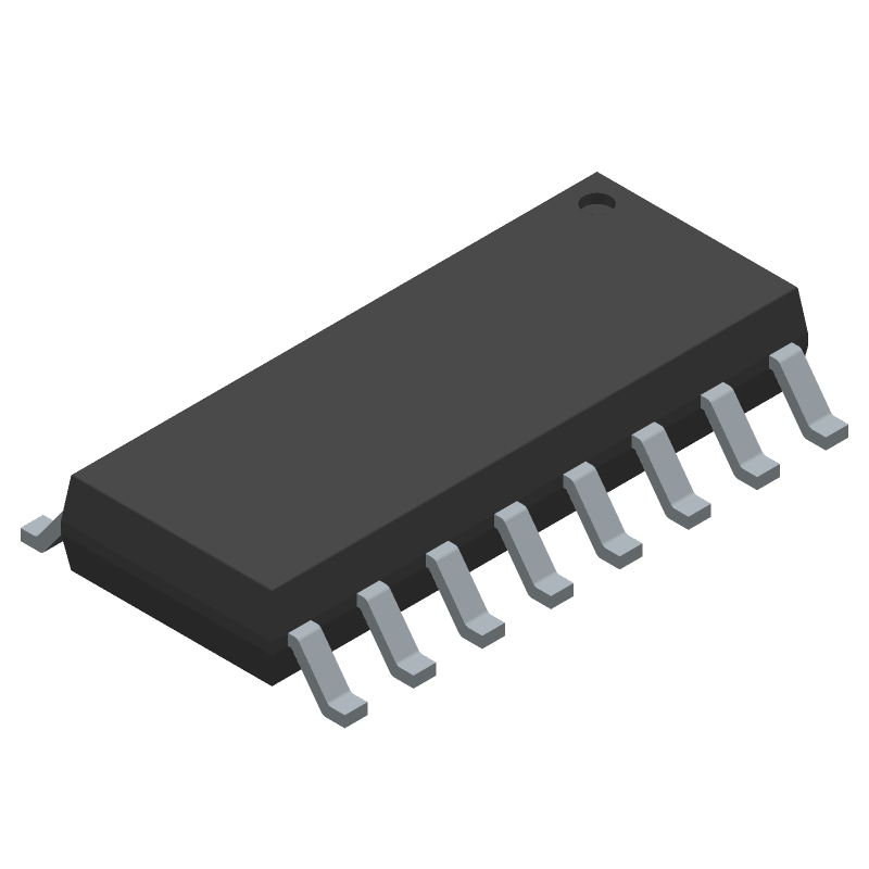
Single-Ended Multiplexer, 1 Func, 8 Channel, CMOS, PDSO16
|
| Pbfree Code | No | |
| Rohs Code | Yes | |
| Part Life Cycle Code | Active | |
| Package Description | 0.150 Inch, Plastic, Sop-16 | |
| Pin Count | 16 | |
| Manufacturer Package Code | 05-08-1610 (S16) | |
| Reach Compliance Code | Compliant | |
| ECCN Code | EAR99 | |
| HTS Code | 8542.39.00.01 | |
| Additional Feature | Can Also Operate With 2.7 V Supply | |
| Analog IC - Other Type | Single-Ended Multiplexer | |
| JESD-30 Code | R-PDSO-G16 | |
| JESD-609 Code | e3 | |
| Length | 9.9 Mm | |
| Moisture Sensitivity Level | 1 | |
| Neg Supply Voltage-Max (Vsup) | -5 V | |
| Neg Supply Voltage-Min (Vsup) | -2.7 V | |
| Neg Supply Voltage-Nom (Vsup) | -5 V | |
| Normal Position | No | |
| Number of Channels | 8 | |
| Number of Functions | 1 | |
| Number of Terminals | 16 | |
| Off-state Isolation-Nom | 70 Db | |
| On-state Resistance Match-Nom | 15 Ω | |
| On-state Resistance-Max (Ron) | 75 Ω | |
| Operating Temperature-Max | 70 °C | |
| Operating Temperature-Min | ||
| Output | Common Output | |
| Package Body Material | Plastic/Epoxy | |
| Package Code | SOP | |
| Package Shape | Rectangular | |
| Package Style | Small Outline | |
| Peak Reflow Temperature (Cel) | 260 | |
| Qualification Status | Not Qualified | |
| Seated Height-Max | 1.75 Mm | |
| Supply Current-Max (Isup) | 0.04 Ma | |
| Supply Voltage-Max (Vsup) | 5 V | |
| Supply Voltage-Min (Vsup) | 2.7 V | |
| Supply Voltage-Nom (Vsup) | 5 V | |
| Surface Mount | Yes | |
| Switch-off Time-Max | 200 Ns | |
| Switch-on Time-Max | 400 Ns | |
| Switching | Break-Before-Make | |
| Technology | Cmos | |
| Temperature Grade | Commercial | |
| Terminal Finish | Matte Tin (Sn) | |
| Terminal Form | Gull Wing | |
| Terminal Pitch | 1.27 Mm | |
| Terminal Position | Dual | |
| Time@Peak Reflow Temperature-Max (s) | 30 | |
| Width | 3.9 Mm |
LTC1391CS#PBF Frequently Asked Questions (FAQ)
-
The recommended layout and placement for the LTC1391CS#PBF involves keeping the analog and digital grounds separate, using a star-ground configuration, and placing the device close to the analog signal sources to minimize noise. Additionally, it's recommended to use a solid ground plane and to keep the device away from high-frequency noise sources.
-
To ensure proper calibration, follow the calibration procedure outlined in the datasheet, which involves applying a known input voltage and adjusting the offset and gain trim pins to achieve the desired accuracy. It's also important to ensure the device is operated within its specified temperature range and that the input signals are within the recommended range.
-
The LTC1391CS#PBF has a limited input signal frequency range of up to 100 kHz and an amplitude range of ±10V. Signals exceeding these limits may result in inaccurate measurements or device damage. It's essential to ensure the input signals are within these limits to ensure accurate and reliable operation.
-
To troubleshoot common issues, start by verifying the input signal is within the recommended range and that the device is properly calibrated. Check the power supply voltage and ensure it's within the recommended range. Also, verify the device is properly connected and that the layout and placement are correct. If issues persist, consult the datasheet and application notes for further guidance.
-
The LTC1391CS#PBF has a maximum operating temperature of 125°C. To ensure reliable operation in high-temperature environments, ensure good thermal conductivity between the device and the PCB, use a heat sink if necessary, and avoid exceeding the maximum power dissipation rating. Additionally, consider using thermal interface materials and following proper PCB design guidelines for thermal management.