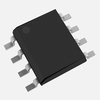
Part Details for ST95040WM6TR by STMicroelectronics
Results Overview of ST95040WM6TR by STMicroelectronics
- Distributor Offerings: (0 listings)
- Number of FFF Equivalents: (0 replacements)
- Tariff Estimator: (Available) NEW
- Number of Functional Equivalents: (0 options)
- CAD Models: (Request Part)
- Part Data Attributes: (Available)
- Reference Designs: (Not Available)
Tip: Data for a part may vary between manufacturers. You can filter for manufacturers on the top of the page next to the part image and part number.
ST95040WM6TR Information
ST95040WM6TR by STMicroelectronics is an EEPROM.
EEPROMs are under the broader part category of Memory Components.
Memory components are essential in electronics for computer processing. They can be volatile or non-volatile, depending on the desired function. Read more about Memory Components on our Memory part category page.
US Tariff Estimator: ST95040WM6TR by STMicroelectronics
Calculations from this tool are estimations only for imports into the United States. Please refer to the distributor or manufacturer and reference official US government sources and authorities to verify any final purchase costs.
ST95040WM6TR Part Data Attributes
|
|
ST95040WM6TR
STMicroelectronics
Buy Now
Datasheet
|
Compare Parts:
ST95040WM6TR
STMicroelectronics
EEPROM, 512X8, Serial, CMOS, PDSO8
|
| Rohs Code | Yes | |
| Part Life Cycle Code | Obsolete | |
| Part Package Code | SOIC | |
| Package Description | 0.150 Inch, Plastic, So-8 | |
| Pin Count | 8 | |
| ECCN Code | EAR99 | |
| HTS Code | 8542.32.00.51 | |
| Clock Frequency-Max (fCLK) | 1 Mhz | |
| Data Retention Time-Min | 40 | |
| Endurance | 1000000 Write/Erase Cycles | |
| JESD-30 Code | R-PDSO-G8 | |
| JESD-609 Code | e4 | |
| Length | 4.9 Mm | |
| Memory Density | 4096 Bit | |
| Memory IC Type | Eeprom | |
| Memory Width | 8 | |
| Number of Functions | 1 | |
| Number of Terminals | 8 | |
| Number of Words | 512 Words | |
| Number of Words Code | 512 | |
| Operating Mode | Synchronous | |
| Operating Temperature-Max | 85 °C | |
| Operating Temperature-Min | -40 °C | |
| Organization | 512x8 | |
| Output Characteristics | 3-State | |
| Package Body Material | Plastic/Epoxy | |
| Package Code | SOP | |
| Package Equivalence Code | SOP8,.25 | |
| Package Shape | Rectangular | |
| Package Style | Small Outline | |
| Parallel/Serial | Serial | |
| Qualification Status | Not Qualified | |
| Seated Height-Max | 1.75 Mm | |
| Serial Bus Type | Spi | |
| Standby Current-Max | 0.000025 A | |
| Supply Current-Max | 0.0015 Ma | |
| Supply Voltage-Max (Vsup) | 5.5 V | |
| Supply Voltage-Min (Vsup) | 2.5 V | |
| Supply Voltage-Nom (Vsup) | 5 V | |
| Surface Mount | Yes | |
| Technology | Cmos | |
| Temperature Grade | Industrial | |
| Terminal Finish | Nickel Palladium Gold | |
| Terminal Form | Gull Wing | |
| Terminal Pitch | 1.27 Mm | |
| Terminal Position | Dual | |
| Width | 3.9 Mm | |
| Write Cycle Time-Max (tWC) | 10 Ms | |
| Write Protection | Hardware/Software |
ST95040WM6TR Frequently Asked Questions (FAQ)
-
STMicroelectronics provides a recommended PCB layout in the application note AN5046, which includes guidelines for thermal pad connection, thermal vias, and copper pouring to ensure optimal thermal performance.
-
The thermal shutdown feature is enabled by default. To handle it, monitor the TSD pin, which goes low when the device reaches the thermal shutdown temperature (typically 150°C). When TSD is low, the device is disabled, and the output voltage is reduced to prevent overheating. Wait for the device to cool down before re-enabling it.
-
The maximum allowed input voltage ripple is not explicitly stated in the datasheet. However, as a general rule, it's recommended to keep the input voltage ripple below 10% of the nominal input voltage to ensure stable operation and prevent oscillations.
-
While the device is rated for operation up to 150°C, it's essential to consider the derating curves provided in the datasheet. For high-temperature applications, ensure that the device is properly heatsinked, and the power dissipation is within the recommended limits to prevent overheating and ensure reliability.
-
The output voltage ripple can be estimated using the formula: ΔVout = (Iout * ESL) / (Cout * fsw), where ESL is the equivalent series inductance of the output capacitor, Cout is the output capacitance, and fsw is the switching frequency. This calculation assumes a simple buck converter topology.