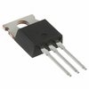
Part Details for STP10NA40 by STMicroelectronics
Results Overview of STP10NA40 by STMicroelectronics
- Distributor Offerings: (2 listings)
- Number of FFF Equivalents: (0 replacements)
- Tariff Estimator: (Not Available)
- Number of Functional Equivalents: (0 options)
- CAD Models: (Request Part)
- Part Data Attributes: (Available)
- Reference Designs: (Not Available)
Tip: Data for a part may vary between manufacturers. You can filter for manufacturers on the top of the page next to the part image and part number.
STP10NA40 Information
STP10NA40 by STMicroelectronics is a Power Field-Effect Transistor.
Power Field-Effect Transistors are under the broader part category of Transistors.
A transistor is a small semiconductor device used to amplify, control, or create electrical signals. When selecting a transistor, factors such as voltage, current rating, gain, and power dissipation must be considered, with common types. Read more about Transistors on our Transistors part category page.
Price & Stock for STP10NA40
| Part # | Distributor | Description | Stock | Price | Buy | |
|---|---|---|---|---|---|---|
|
|
Quest Components | POWER FIELD-EFFECT TRANSISTOR, 10A I(D), 400V, 0.55OHM, 1-ELEMENT, N-CHANNEL, SILICON, METAL-OXIDE SEMICONDUCTOR FET, TO-220AB | 10 |
|
Buy Now | |
|
|
Unikey Electronic Pte Ltd | Min Qty: 163 Date Code: 99+ | 715 |
|
$1.6704 / $3.0798 | Buy Now |
STP10NA40 Part Data Attributes
|
|
STP10NA40
STMicroelectronics
Buy Now
Datasheet
|
Compare Parts:
STP10NA40
STMicroelectronics
Power Field-Effect Transistor, 10A I(D), 400V, 0.55ohm, 1-Element, N-Channel, Silicon, Metal-oxide Semiconductor FET, TO-220AB
|
| Pbfree Code | Yes | |
| Rohs Code | Yes | |
| Part Life Cycle Code | Active Unconfirmed | |
| Part Package Code | TO-220AB | |
| Package Description | To-220, 3 Pin | |
| Pin Count | 3 | |
| Similar Group | Tr0810021002yyyy10059067 | |
| ECCN Code | EAR99 | |
| Avalanche Energy Rating (Eas) | 500 Mj | |
| Configuration | Single With Built-In Diode | |
| DS Breakdown Voltage-Min | 400 V | |
| Drain Current-Max (ID) | 10 A | |
| Drain-source On Resistance-Max | 0.55 Ω | |
| FET Technology | Metal-Oxide Semiconductor | |
| Feedback Cap-Max (Crss) | 10 Pf | |
| JEDEC-95 Code | TO-220AB | |
| JESD-30 Code | R-PSFM-T3 | |
| JESD-609 Code | e3 | |
| Number of Elements | 1 | |
| Number of Terminals | 3 | |
| Operating Mode | Enhancement Mode | |
| Operating Temperature-Max | 150 °C | |
| Package Body Material | Plastic/Epoxy | |
| Package Shape | Rectangular | |
| Package Style | Flange Mount | |
| Polarity/Channel Type | N-Channel | |
| Power Dissipation-Max (Abs) | 125 W | |
| Pulsed Drain Current-Max (IDM) | 40 A | |
| Qualification Status | Not Qualified | |
| Surface Mount | No | |
| Terminal Finish | Matte Tin (Sn) | |
| Terminal Form | Through-Hole | |
| Terminal Position | Single | |
| Transistor Application | Switching | |
| Transistor Element Material | Silicon |
STP10NA40 Frequently Asked Questions (FAQ)
-
The maximum operating temperature range for the STP10NA40 is -40°C to 150°C, as specified in the datasheet. However, it's recommended to operate the device within a temperature range of -40°C to 125°C for optimal performance and reliability.
-
To ensure proper biasing, make sure to follow the recommended voltage and current ratings specified in the datasheet. Additionally, ensure that the input and output pins are properly terminated, and that the device is operated within the recommended operating conditions.
-
For optimal thermal management, it's recommended to use a multi-layer PCB with a solid ground plane and to place the device on a thermal pad. Ensure that the PCB layout allows for good heat dissipation and that the device is not exposed to excessive thermal stress.
-
The STP10NA40 has built-in ESD protection, but it's still recommended to follow proper ESD handling procedures during assembly and testing. Use ESD-safe materials, handle the device by the body or pins, and avoid touching the pins or leads.
-
Follow the recommended test and measurement procedures outlined in the datasheet, including using a proper test fixture and ensuring that the device is properly biased and terminated. Additionally, use a high-impedance probe or a low-capacitance probe to minimize loading effects.