| Part Number | Manufacturer | Composite Price | Description | Compare |
|---|---|---|---|---|
| TLC5615CDR | Texas Instruments | $2.5116 | D/A Converter, 1 Func, Serial Input Loading, 12.5us Settling Time, PDSO8 | TLC5615ID vs TLC5615CDR |
| TLC5615IDR | Texas Instruments | $2.6916 | D/A Converter, 1 Func, Serial Input Loading, 12.5us Settling Time, PDSO8 | TLC5615ID vs TLC5615IDR |
| TLC5615CDG4 | Texas Instruments | Check for Price | D/A Converter, 1 Func, Serial Input Loading, 12.5us Settling Time, PDSO8 | TLC5615ID vs TLC5615CDG4 |
| TLC5615IDRG4 | Texas Instruments | Check for Price | D/A Converter, 1 Func, Serial Input Loading, 12.5us Settling Time, PDSO8 | TLC5615ID vs TLC5615IDRG4 |
Part Details for TLC5615ID by Texas Instruments
Results Overview of TLC5615ID by Texas Instruments
- Distributor Offerings: (4 listings)
- Number of FFF Equivalents: (4 replacements)
- Tariff Estimator: (Available) NEW
- Number of Functional Equivalents: (5 options)
- CAD Models: (Available)
- Part Data Attributes: (Available)
- Reference Designs: (Not Available)
Tip: Data for a part may vary between manufacturers. You can filter for manufacturers on the top of the page next to the part image and part number.
Applications
Education and Research
Environmental Monitoring
Industrial Automation
Agriculture Technology
Medical Imaging
TLC5615ID Information
TLC5615ID by Texas Instruments is a Digital to Analog Converter.
Digital to Analog Converters are under the broader part category of Converters.
A converter is an electrical circuit that transforms electric energy into a different form that will support a elecrical load needed by a device. Read more about Converters on our Converters part category page.
Available Datasheets
| Part # | Manufacturer | Description | Datasheet |
|---|---|---|---|
| TLC5615ID | Texas Instruments | 10-bit, single-channel, low-power DAC with 12.5us settling time and power-on reset 8-SOIC -40 to 85 | |
| TLC5615IDGK | Texas Instruments | 10-bit, single-channel, low-power DAC with 12.5us settling time and power-on reset 8-VSSOP -40 to 85 | |
| TLC5615IDR | Texas Instruments | 10-bit, single-channel, low-power DAC with 12.5us settling time and power-on reset 8-SOIC -40 to 85 |
Price & Stock for TLC5615ID
| Part # | Distributor | Description | Stock | Price | Buy | |
|---|---|---|---|---|---|---|
|
DISTI #
595-TLC5615ID
|
Mouser Electronics | Digital to Analog Converters - DAC 10bit DAC A 595-TLC5 615IDR A 595-TLC561 A 595-TLC5615IDR RoHS: Compliant | 221 |
|
$6.8000 / $11.2400 | Buy Now |
|
|
Quest Components | SERIAL INPUT LOADING, 12.5 US SETTLING TIME, 10-BIT DAC, PDSO8 | 129 |
|
$3.5295 / $8.1450 | Buy Now |
|
|
Rochester Electronics | IC VOLT REG Adjustable 1 REG -1.25V 500mA 8-SOIC Tube RoHS: Compliant Status: Active Min Qty: 1 | 1 |
|
$5.0700 / $6.3400 | Buy Now |
|
|
Vyrian | D/A Converter, 1 Func, Serial Input Loading, 12.5us Settling Time, PDSO8 | 8539 |
|
RFQ |
US Tariff Estimator: TLC5615ID by Texas Instruments
Calculations from this tool are estimations only for imports into the United States. Please refer to the distributor or manufacturer and reference official US government sources and authorities to verify any final purchase costs.
TLC5615ID CAD Models
-
Part Symbol
-
Footprint
-
3D Model
Available Download Formats
By downloading CAD models, you agree to our Terms & Conditions and Privacy Policy
TLC5615ID Part Data Attributes
|
|
TLC5615ID
Texas Instruments
Buy Now
Datasheet
|
Compare Parts:
TLC5615ID
Texas Instruments
D/A Converter, 1 Func, Serial Input Loading, 12.5us Settling Time, PDSO8
|
| Pbfree Code | Yes | |
| Rohs Code | Yes | |
| Part Life Cycle Code | Active | |
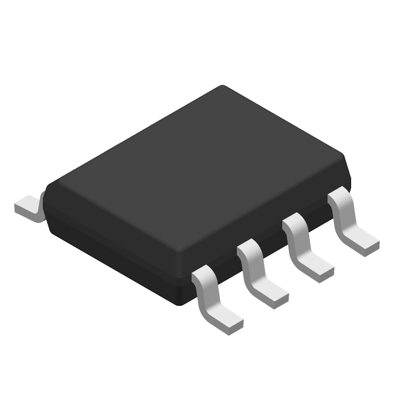
| Part Package Code | SOIC | |
| Package Description | Soic-8 | |
| Pin Count | 8 | |
| ECCN Code | EAR99 | |
| HTS Code | 8542.39.00.40 | |
| Analog Output Voltage-Max | 5.1 V | |
| Analog Output Voltage-Min | ||
| Converter Type | D/A Converter | |
| Input Bit Code | BINARY | |
| Input Format | Serial | |
| JESD-30 Code | R-PDSO-G8 | |
| JESD-609 Code | e4 | |
| Length | 4.9 Mm | |
| Linearity Error-Max (EL) | 0.0977% | |
| Moisture Sensitivity Level | 1 | |
| Number of Bits | 10 | |
| Number of Functions | 1 | |
| Number of Terminals | 8 | |
| Operating Temperature-Max | 85 °C | |
| Operating Temperature-Min | -40 °C | |
| Package Body Material | Plastic/Epoxy | |
| Package Code | SOP | |
| Package Equivalence Code | SOP8,.25 | |
| Package Shape | Rectangular | |
| Package Style | Small Outline | |
| Packing Method | Tube | |
| Peak Reflow Temperature (Cel) | 260 | |
| Qualification Status | Not Qualified | |
| Sample Rate | 0.075 Mhz | |
| Seated Height-Max | 1.75 Mm | |
| Settling Time-Max | 12.5 µS | |
| Settling Time-Nom (tstl) | 12.5 µS | |
| Supply Current-Max | 0.35 Ma | |
| Supply Voltage-Nom | 5 V | |
| Surface Mount | Yes | |
| Technology | Cmos | |
| Temperature Grade | Industrial | |
| Terminal Finish | Nickel/Palladium/Gold (Ni/Pd/Au) | |
| Terminal Form | Gull Wing | |
| Terminal Pitch | 1.27 Mm | |
| Terminal Position | Dual | |
| Time@Peak Reflow Temperature-Max (s) | 30 | |
| Width | 3.9 Mm |
Alternate Parts for TLC5615ID
This table gives cross-reference parts and alternative options found for TLC5615ID. The Form Fit Function (FFF) tab will give you the options that are more likely to serve as direct pin-to-pin alternates or drop-in parts. The Functional Equivalents tab will give you options that are likely to match the same function of TLC5615ID, but it may not fit your design. Always verify details of parts you are evaluating, as these parts are offered as suggestions for what you are looking for and are not guaranteed.
TLC5615ID Frequently Asked Questions (FAQ)
-
The recommended power-on sequence is to apply VCC first, followed by VREF, and then the analog input signal. This sequence helps prevent unwanted voltage transients and ensures proper device operation.
-
To ensure accurate voltage reference output, it's essential to decouple the VREF pin with a 0.1uF capacitor to GND, and use a low-impedance voltage source for VCC. Additionally, keep the VREF pin away from noise sources and ensure good PCB layout practices.
-
The TLC5615ID can drive up to 10nF of capacitive load. Exceeding this limit may cause instability or oscillations in the device. If a larger capacitive load is required, consider adding a buffer amplifier or using a device with higher drive capability.
-
To minimize noise and EMI, use a multi-layer PCB with a solid ground plane, keep signal traces short and away from noise sources, and use shielding or guard rings around sensitive signals. Additionally, consider using a low-pass filter or ferrite beads to filter out high-frequency noise.
-
The TLC5615ID has a thermal derating curve of 5.5mW/°C above 25°C. This means that for every degree above 25°C, the maximum power dissipation decreases by 5.5mW. Ensure proper thermal management and heat sinking to maintain reliable device operation.