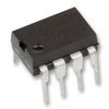
Part Details for ST93C56B1 by STMicroelectronics
Results Overview of ST93C56B1 by STMicroelectronics
- Distributor Offerings: (1 listing)
- Number of FFF Equivalents: (0 replacements)
- Tariff Estimator: (Available) NEW
- Number of Functional Equivalents: (0 options)
- CAD Models: (Available)
- Part Data Attributes: (Available)
- Reference Designs: (Not Available)
Tip: Data for a part may vary between manufacturers. You can filter for manufacturers on the top of the page next to the part image and part number.
ST93C56B1 Information
ST93C56B1 by STMicroelectronics is an EEPROM.
EEPROMs are under the broader part category of Memory Components.
Memory components are essential in electronics for computer processing. They can be volatile or non-volatile, depending on the desired function. Read more about Memory Components on our Memory part category page.
Price & Stock for ST93C56B1
| Part # | Distributor | Description | Stock | Price | Buy | |
|---|---|---|---|---|---|---|
|
|
Quest Components | EEPROM, 128X16, SERIAL, CMOS, PDIP8 | 24469 |
|
$0.4410 / $1.2600 | Buy Now |
US Tariff Estimator: ST93C56B1 by STMicroelectronics
Calculations from this tool are estimations only for imports into the United States. Please refer to the distributor or manufacturer and reference official US government sources and authorities to verify any final purchase costs.
ST93C56B1 CAD Models
-
Part Symbol
-
Footprint
-
3D Model
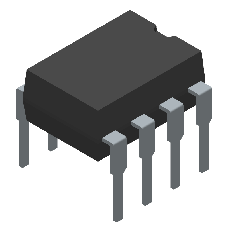
Available Download Formats
By downloading CAD models, you agree to our Terms & Conditions and Privacy Policy
ST93C56B1 Part Data Attributes
|
|
ST93C56B1
STMicroelectronics
Buy Now
Datasheet
|
Compare Parts:
ST93C56B1
STMicroelectronics
EEPROM, 128X16, Serial, CMOS, PDIP8
|
| Part Life Cycle Code | Obsolete | |
| Part Package Code | DIP | |
| Package Description | Plastic, Dip-8 | |
| Pin Count | 8 | |
| ECCN Code | EAR99 | |
| HTS Code | 8542.32.00.51 | |
| Additional Feature | Microwire Bus Interface; Automatic Write; 1000k Erase/Write Cycles Min.; Data Retention > 10 Years | |
| Alternate Memory Width | 8 | |
| Clock Frequency-Max (fCLK) | 1 Mhz | |
| Data Retention Time-Min | 40 | |
| Endurance | 1000000 Write/Erase Cycles | |
| JESD-30 Code | R-PDIP-T8 | |
| JESD-609 Code | e0 | |
| Length | 9.55 Mm | |
| Memory Density | 2048 Bit | |
| Memory IC Type | Eeprom | |
| Memory Width | 16 | |
| Number of Functions | 1 | |
| Number of Terminals | 8 | |
| Number of Words | 128 Words | |
| Number of Words Code | 128 | |
| Operating Mode | Synchronous | |
| Operating Temperature-Max | 70 °C | |
| Operating Temperature-Min | ||
| Organization | 128x16 | |
| Output Characteristics | 3-State | |
| Package Body Material | Plastic/Epoxy | |
| Package Code | DIP | |
| Package Equivalence Code | DIP8,.3 | |
| Package Shape | Rectangular | |
| Package Style | In-Line | |
| Parallel/Serial | Serial | |
| Qualification Status | Not Qualified | |
| Seated Height-Max | 4.8 Mm | |
| Serial Bus Type | Microwire | |
| Standby Current-Max | 0.00005 A | |
| Supply Current-Max | 0.003 Ma | |
| Supply Voltage-Max (Vsup) | 5.5 V | |
| Supply Voltage-Min (Vsup) | 4.5 V | |
| Supply Voltage-Nom (Vsup) | 5 V | |
| Surface Mount | No | |
| Technology | Cmos | |
| Temperature Grade | Commercial | |
| Terminal Finish | Tin/Lead (Sn/Pb) | |
| Terminal Form | Through-Hole | |
| Terminal Pitch | 2.54 Mm | |
| Terminal Position | Dual | |
| Width | 7.62 Mm | |
| Write Cycle Time-Max (tWC) | 10 Ms | |
| Write Protection | Software |
ST93C56B1 Frequently Asked Questions (FAQ)
-
The ST93C56B1 has a minimum of 100,000 write cycles, but the actual number of write cycles may vary depending on the operating conditions and usage patterns.
-
The HOLD pin should be pulled high during power-up and power-down to prevent any unwanted writes or reads. It's recommended to use an external pull-up resistor to ensure the pin is at a valid logic level.
-
The recommended clock frequency for the ST93C56B1 is up to 3.4 MHz, but it can operate at frequencies up to 5 MHz with some limitations. It's essential to consult the datasheet for specific frequency-related limitations.
-
To ensure data integrity during power failures, it's recommended to use a capacitor or a battery-backed solution to maintain power to the device during the power-down sequence. This allows the device to complete any ongoing write operations and prevent data corruption.
-
The WP (Write Protect) pin is used to prevent writes to the entire memory array or specific blocks. When the WP pin is pulled low, the device enters a write-protected state, and any write attempts will be ignored. The WP pin can be used to protect sensitive data or configuration settings.